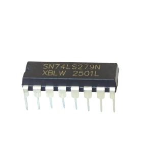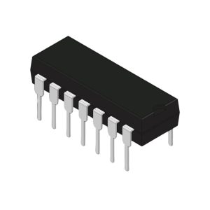






7406 Hex Inverter Buffer/Driver IC
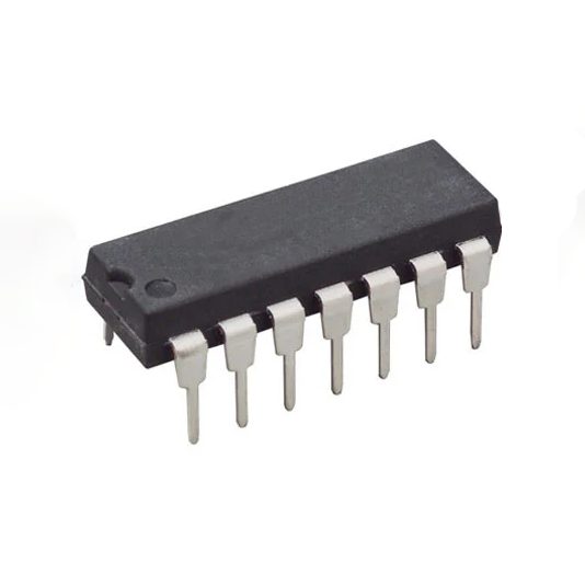
The 7406 is a six-channel hex inverter buffer/driver IC commonly used for signal inversion, logic interfacing, and driving higher-voltage or higher-current loads.
13.00 EGP
In stockSKU 300000011712
Buy Now
Shipping across EgyptDelivered to your door
Cash on deliveryPay when your order arrives
Not sure it fits your project?Ask us on WhatsApp - we reply fast
7406 Hex Inverter Buffer/Driver IC
The 7406 (ex 74LS06) is a chip with six open-collector inverters that has a maximum output voltage of 30V and a sink current of 40 mA so that they can interface with high-level circuits (such as MOSFETs), or for driving high-current loads.
When you have an open collector output, it means it’s easy to connect it to other chips that use different logic levels. However, it also means you can’t just swap it out with a regular inverter chip.
Features:
- Six independent inverter channels.
- Open-collector outputs.
- High-voltage output capability.
- High sink-current capability.
- Suitable for logic-level interfacing.
- Individual operation of each inverter.
- TTL-compatible inputs.
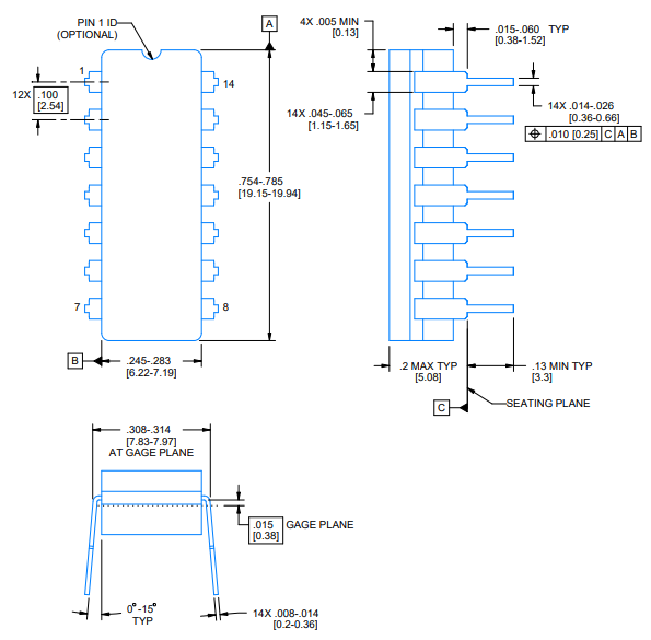
- 14-pin through-hole package.
How To Use This Chip
The 74LS06 comes in a 14-pin package, and you need to connect it to power before you can use it. Most 7400 ICs support a VCC voltage of 5V. One difference between the HC and LS versions of the chip is that the 74HC06 supports 2V to 6V, while the 74LS06 only supports 5V.
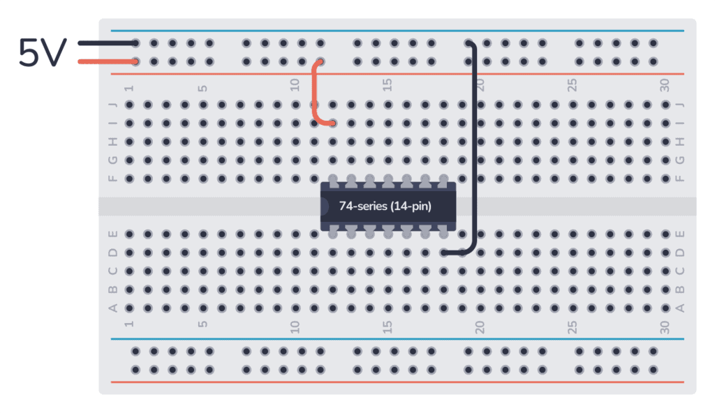
Pinout

| Pin # | Type | Description |
|---|---|---|
| 1 | Input | Input to the first NOT gate. |
| 2 | Output | Open-collector output from the first NOT gate. |
| 3 | Input | Input to the second NOT gate. |
| 4 | Output | Open-collector output from the second NOT gate. |
| 5 | Input | Input to the third NOT gate. |
| 6 | Output | Open-collector output from the third NOT gate. |
| 7 | Power | Connect to ground (GND). |
| 8 | Output | Open-collector output from the fourth NOT gate. |
| 9 | Input | Input to the fourth NOT gate. |
| 10 | Output | Open-collector output from the fifth NOT gate. |
| 11 | Input | Input to the fifth NOT gate. |
| 12 | Output | Open-collector output from the sixth NOT gate. |
| 13 | Input | Input to the sixth NOT gate. |
| 14 | Power | Positive power supply (VCC). Connect to +5V power. |
Technical Specifications
| Physical | |
| Case/Package | PDIP |
| Mount | Through Hole |
| Number of Pins | 14 |
| Technical | |
| High Level Output Current | -250 µA |
| Logic Function | Buffer, Inverter, Inverting |
| Low Level Output Current | 40 mA |
| Max Operating Temperature | 70 °C |
| Max Supply Voltage | 5.25 V |
| Min Operating Temperature | 0 °C |
| Min Supply Voltage | 4.75 V |
| Nominal Supply Current | 100 µA |
| Number of Bits | 6 |
| Number of Channels | 6 |
| Number of Circuits | 6 |
| Number of Elements | 6 |
| Number of Gates | 6 |
| Number of Input Lines | 6 |
| Number of Inputs | 1 |
| Number of Output Lines | 6 |
| Number of Outputs | 6 |
| Operating Supply Current | 100 µA |
| Operating Supply Voltage | 5 V |
| Polarity | Inverting |
| Propagation Delay | 20 ns |
| Schmitt Trigger Input | No |
| Termination | Through Hole |
| Turn-On Delay Time | 20 ns |

Applications:
- Logic signal inversion.
- TTL signal buffering.
- Logic-level conversion.
- MOS interface circuits.
- Relay driving.
- Indicator lamp driving.
- High-current digital signal switching.
- Open-collector logic circuits.
- Digital control systems.
- Microprocessor and digital interface circuits.
Packages Included:
- 1 × 7406 Hex Inverter Buffer/Driver IC.
7406 Datasheet
Related products