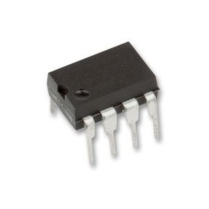



TL072CN Dual Operational Amplifier IC ±18V 1.4mA DIP-8
Low noise J-FET dual op-amp, ±18V supply, 16V/µs slew rate, 4MHz GBP, 15nV/√Hz noise, DIP-8 package
8.00 EGP
Buy NowTL072 Operational Amplifier DIP-8
The TL072CN from STMicroelectronics is a low-noise, high-speed J-FET input dual operational amplifier, built as a monolithic integrated circuit incorporating well-matched, high-voltage J-FET and bipolar transistors. In the order code TL072CN, the letter “C” designates the commercial temperature grade (0 °C to +70 °C) and the letter “N” designates the 8-pin plastic DIP package (DIP-8).
The J-FET input stage gives the TL072CN a very high input impedance of 10¹² Ω, together with low input bias and offset currents (20 pA and 5 pA typ at 25 °C) and a low offset voltage temperature coefficient (10 µV/°C). It combines a high slew rate of 16 V/µs (typ) with a typical gain bandwidth product of 4 MHz, while keeping noise down to 15 nV/√Hz and total harmonic distortion to just 0.01% (typ), with 120 dB channel separation between the two amplifiers.
Features
- Wide common-mode (up to VCC+) and differential voltage range
- Low input bias and offset current
- Low noise: eₙ = 15 nV/√Hz (typ)
- Output short-circuit protection
- High input impedance J-FET input stage (10¹² Ω)
- Low harmonic distortion: 0.01% (typ)
- Internal frequency compensation
- Latch-up free operation
- High slew rate: 16 V/µs (typ)
Specifications
| Parameter | Value |
|---|---|
| GENERAL INFORMATION | |
| Part Number | TL072CN |
| Device Type | Low Noise J-FET Dual Operational Amplifier |
| Manufacturer | STMicroelectronics |
| Package | DIP-8 (8-Pin Plastic Dual In-line Package, order suffix “N”) |
| Number of Amplifiers | 2 (Dual) |
| Operating Temperature Range | 0°C to +70°C (Commercial grade, suffix “C”) |
| Storage Temperature Range | −65°C to +150°C |
| ABSOLUTE MAXIMUM RATINGS | |
| Supply Voltage (VCC) | ±18 V |
| Input Voltage (Vi) | ±15 V |
| Differential Input Voltage (Vid) | ±30 V |
| Power Dissipation (Ptot) | 680 mW |
| Output Short-Circuit Duration | Infinite |
| ELECTRICAL CHARACTERISTICS (VCC = ±15 V, Tamb = 25°C, unless otherwise specified) | |
| Input Offset Voltage (Vio, RS = 50 Ω) | 3 mV (typ), 10 mV (max); 13 mV (max over full temperature range) |
| Input Offset Voltage Drift | 10 µV/°C |
| Input Offset Current (Iio) | 5 pA (typ), 100 pA (max) |
| Input Bias Current (Iib) | 20 pA (typ), 200 pA (max) |
| Large Signal Voltage Gain (Avd, RL = 2 kΩ, VO = ±10 V) | 25 V/mV (min), 200 V/mV (typ) |
| Supply Voltage Rejection Ratio (SVR, RS = 50 Ω) | 70 dB (min), 86 dB (typ) |
| Supply Current per Amplifier (ICC, no load) | 1.4 mA (typ), 2.5 mA (max) |
| Input Common-Mode Voltage Range (Vicm) | ±11 V (min); −12 V to +15 V |
| Common-Mode Rejection Ratio (CMR, RS = 50 Ω) | 70 dB (min), 86 dB (typ) |
| Output Short-Circuit Current (Ios) | 10 mA (min), 40 mA (typ), 60 mA (max) |
| Output Voltage Swing (±VOPP) | ±10 V (min) / ±12 V (typ) at RL = 2 kΩ; ±12 V (min) / ±13.5 V (typ) at RL = 10 kΩ |
| Slew Rate (SR) | 8 V/µs (min), 16 V/µs (typ) |
| Rise Time (tr) | 0.1 µs |
| Overshoot (KOV) | 10 % |
| Gain Bandwidth Product (GBP) | 2.5 MHz (min), 4 MHz (typ) |
| Input Resistance (Ri) | 1012 Ω (1 TΩ) |
| Total Harmonic Distortion (THD, f = 1 kHz) | 0.01 % (typ) |
| Equivalent Input Noise Voltage (en, f = 1 kHz, RS = 100 Ω) | 15 nV/√Hz |
| Phase Margin (Φm) | 45° |
| Channel Separation (VO1/VO2, AV = 100) | 120 dB |
| PIN CONFIGURATION (DIP-8, TOP VIEW) | |
| Pin 1 | Output 1 |
| Pin 2 | Inverting Input 1 (−) |
| Pin 3 | Non-Inverting Input 1 (+) |
| Pin 4 | VCC− (Negative Supply) |
| Pin 5 | Non-Inverting Input 2 (+) |
| Pin 6 | Inverting Input 2 (−) |
| Pin 7 | Output 2 |
| Pin 8 | VCC+ (Positive Supply) |

Applications
- 100 kHz quadrature (sine/cosine) oscillator
- General-purpose dual op-amp circuits
Package Content
- 1 x TL072CN Dual Operational Amplifier IC ±18V 1.4mA DIP-8
DataSheet
Related products