CD4049 Pinout Configuration
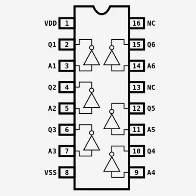
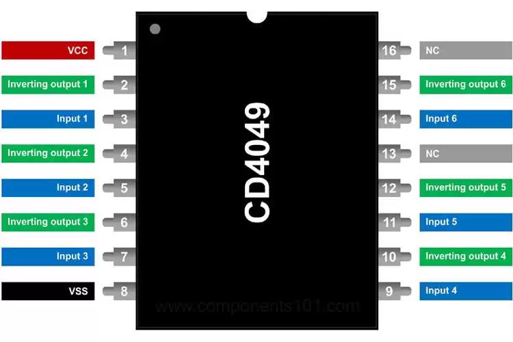
The CD4049 IC has 16 pins for Input and Output for inverting the signals. The table below describes the pin configuration of the NOT gate IC.
| Pin Number | Pin Type | Description/Direction |
| 1 | VCC | Positive input supply |
| 2 | G | Inverting output 1 |
| 3 | A | Input 1 |
| 4 | H | Inverting output 2 |
| 5 | B | Input 2 |
| 6 | I | Inverting output 3 |
| 7 | C | Input 3 |
| 8 | VSS | Negative Supply |
| 9 | D | Input 4 |
| 10 | J | Inverting output 4 |
| 11 | E | Input 5 |
| 12 | K | Inverting output 5 |
| 13 | NC | No connection |
| 14 | F | Input 6 |
| 15 | L | Inverting output 6 |
| 16 | NC | No connection |
Product Attributes
| TYPE | DESCRIPTION |
| Category | Integrated Circuits (ICs) Logic Gates and Inverters |
| Series | 4000B |
| Logic Type | Inverter |
| Number of Circuits | 6 |
| Number of Inputs | 1 |
| Features | – |
| Voltage – Supply | 3V ~ 18V |
| Current – Quiescent (Max) | 4 µA |
| Current – Output High, Low | 4.3mA, 24mA |
| Input Logic Level – Low | 1V ~ 2.5V |
| Input Logic Level – High | 4V ~ 12.5V |
| Max Propagation Delay @ V, Max CL | 50ns @ 15V, 50pF |
| Operating Temperature | -55°C ~ 125°C |
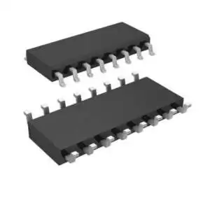
| Mounting Type | Surface Mount |
| Supplier Device Package | 16-SOIC |
| Package / Case | 16-SOIC (0.154″, 3.90mm Width) |
| Base Product Number | CD4049 |


Reviews
There are no reviews yet.