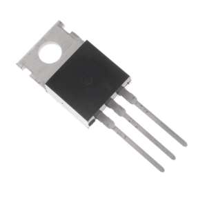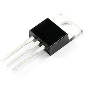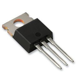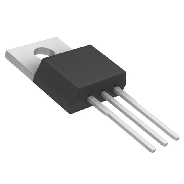
FDP120N10 N-Channel Power MOSFET 100V 74A TO-220
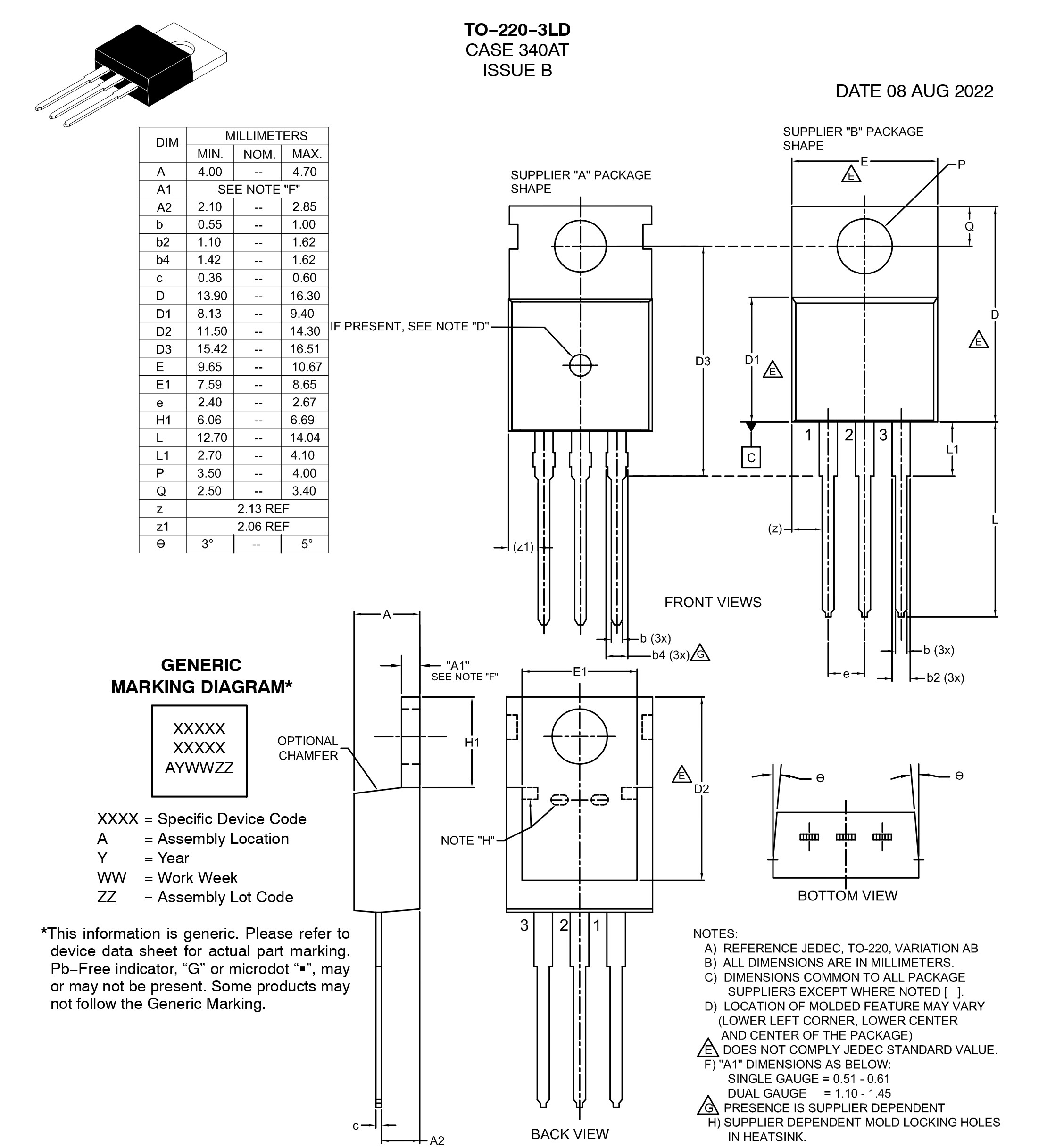
The FDP120N10 is a high-performance N-Channel MOSFET produced using advanced POWERTRENCH process. This process has been tailored to minimize on-state resistance while maintaining superior switching performance. With a 100 V drain-to-source breakdown voltage and 74 A continuous drain current at TC = 25°C, the FDP120N10 is suitable for high-current power applications. Its typical on-resistance is 9.7 mΩ at VGS = 10 V and ID = 74 A, with a maximum specified RDS(on) of 12 mΩ under the same conditions. The device is supplied in a TO-220 package, case style 340AT, and is Pb-Free, Halide Free, and RoHS Compliant. It is designed for applications including synchronous rectification, battery protection, motor drives, UPS systems, and micro solar inverters.
Features
- N-Channel POWERTRENCH MOSFET
- 100 V drain-source voltage, VDSS
- 74 A continuous drain current at TC = 25°C, silicon limited
- 52 A continuous drain current at TC = 100°C, silicon limited
- 296 A pulsed drain current
- Typical RDS(on): 9.7 mΩ @ VGS = 10 V, ID = 74 A
- Maximum RDS(on): 12 mΩ @ VGS = 10 V, ID = 74 A
- Fast switching speed
- Low gate charge
- High-performance trench technology for extremely low RDS(on)
- High power and current handling capability
- Gate threshold voltage: 2.5 V to 4.5 V
- Total gate charge: 66 nC typical, 86 nC maximum at VGS = 10 V
Specifications
Absolute Maximum Ratings (TC = 25°C unless otherwise noted)
| Parameter | Symbol | Rating | Unit |
|---|---|---|---|
| Drain to Source Voltage | VDSS | 100 | V |
| Gate to Source Voltage | VGSS | ±20 | V |
| Continuous Drain Current (TC = 25°C, Silicon Limited) | ID | 74 | A |
| Continuous Drain Current (TC = 100°C, Silicon Limited) | ID | 52 | A |
| Pulsed Drain Current | IDM | 296 | A |
| Single Pulsed Avalanche Energy (L = 0.11 mH, IAS = 60 A) | EAS | 198 | mJ |
| Peak Diode Recovery dv/dt | dv/dt | 6.0 | V/ns |
| Power Dissipation (TC = 25°C) | PD | 170 | W |
| Power Dissipation Derating Linearly Above 25°C | – | 1.14 | W/°C |
| Operating and Storage Temperature Range | TJ, TSTG | -55 to +175 | °C |
| Maximum Lead Temperature for Soldering (1/8″ from Case for 5s) | TL | 300 | °C |
Thermal Characteristics
| Parameter | Symbol | Max | Unit |
|---|---|---|---|
| Thermal Resistance, Junction to Case | RθJC | 0.88 | °C/W |
| Thermal Resistance, Junction to Ambient | RθJA | 62.5 | °C/W |
Electrical Characteristics (TC = 25°C)
| Parameter | Symbol | Test Conditions | Min | Typ | Max | Unit |
|---|---|---|---|---|---|---|
| Drain to Source Breakdown Voltage | BVDSS | ID = 250 µA, VGS = 0V | 100 | – | – | V |
| Breakdown Voltage Temp. Coefficient | ΔBVDSS / ΔTJ | ID = 250 µA, Ref. to 25°C | – | 0.1 | – | V/°C |
| Zero Gate Voltage Drain Current | IDSS | VDS = 100V, VGS = 0V | – | – | 1 | µA |
| Gate to Body Leakage Current | IGSS | VGS = ±20V, VDS = 0V | – | – | ±100 | nA |
| Gate Threshold Voltage | VGS(th) | VGS = VDS, ID = 250 µA | 2.5 | – | 4.5 | V |
| Static Drain to Source On-Resistance | RDS(on) | VGS = 10V, ID = 74A | – | 9.7 | 12.0 | mΩ |
| Forward Transconductance | gFS | VDS = 10V, ID = 74A | – | 105 | – | S |
Dynamic & Switching Characteristics
| Parameter | Symbol | Test Conditions | Min | Typ | Max | Unit |
|---|---|---|---|---|---|---|
| Input Capacitance | Ciss | VDS = 25V, VGS = 0V, f = 1 MHz | – | 4215 | 5605 | pF |
| Output Capacitance | Coss | – | 405 | 540 | pF | |
| Reverse Transfer Capacitance | Crss | – | 170 | 255 | pF | |
| Total Gate Charge at 10V | Qg(tot) | VDS = 80V, ID = 74A, VGS = 10V | – | 66 | 86 | nC |
| Gate to Source Gate Charge | Qgs | – | 26 | – | nC | |
| Gate to Drain “Miller” Charge | Qgd | – | 20 | – | nC | |
| Turn-On Delay Time | td(on) | VDD = 50V, ID = 74A, VGS = 10V, RG = 4.7 Ω | – | 27 | 64 | ns |
| Turn-On Rise Time | tr | – | 105 | 220 | ns | |
| Turn-Off Delay Time | td(off) | – | 39 | 88 | ns | |
| Turn-Off Fall Time | tf | – | 15 | 40 | ns |
Drain-Source Diode Characteristics
| Parameter | Symbol | Test Conditions | Min | Typ | Max | Unit |
|---|---|---|---|---|---|---|
| Max Continuous Diode Forward Current | IS | – | – | – | 74 | A |
| Max Pulsed Diode Forward Current | ISM | – | – | – | 296 | A |
| Drain to Source Diode Forward Voltage | VSD | VGS = 0V, ISD = 74A | – | – | 1.3 | V |
| Reverse Recovery Time | trr | VGS = 0V, ISD = 74A, dIF/dt = 100 A/µs | – | 44 | – | ns |
| Reverse Recovery Charge | Qrr | – | 67 | – | nC |
Applications
- Synchronous rectification for ATX / server / telecom PSU
- Battery protection circuits
- Motor drives
- Uninterruptible power supplies, UPS
- Micro solar inverters
Package Content
- 1 x FDP120N10 N-Channel Power MOSFET 100V 74A TO-220