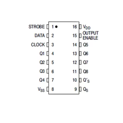
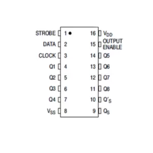
CD4094 Pinout
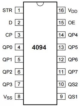
| Pin No | Pin Name | Description |
|---|---|---|
| 1 | STROBE | Strobe Pin |
| 2 | DATA | Serial Data Input Pin |
| 3 | CLOCK | Shift Register Clock Pin |
| 4 | Q1 | Shift Register Output Pin 1 |
| 5 | Q2 | Shift Register Output Pin 2 |
| 6 | Q3 | Shift Register Output Pin 3 |
| 7 | Q4 | Shift Register Output Pin 4 |
| 8 | VSS | Source Supply |
| 9 | Qs | Store Register Output |
| 10 | Q’s | Store Register Inverted Output |
| 11 | Q8 | Shift Register Output Pin 8 |
| 12 | Q7 | Shift Register Output Pin 7 |
| 13 | Q6 | Shift Register Output Pin 6 |
| 14 | Q5 | Shift Register Output Pin 5 |
| 15 | ENB-OUT | enables outputs if set high |
| 16 | VDD | Drain Supply |
Features:-
- High Voltage Type (20V Rating)
- 3-State Parallel Outputs for Connection to Common Bus
- Separate Serial Outputs Synchronous to Both Positive and Negative Clock Edges for Cascading
- Medium Speed Operation – 5MHz at 10V (type)
- Quiescent Current at 20V
- Maximum Input Current of 1µA at 18V Over Full Package Temperature Range; 100nA at 18V and +25oC
- Noise Margin (Over Full Package/Temperature Range) – 1V at VDD = 5V – 2V at VDD = 10V – 2.5V at VDD = 15V
- 5V, 10V and 15V Parametric Ratings
Specifications
| Product Attribute | Attribute Value |
| Product Category: | Counter Shift Registers |
| Counting Sequence: | Serial to Serial/Parallel |
| Number of Circuits: | 2 |
| Number of Bits: | 8 bit |
| Package/Case: | PDIP-16 |
| Logic Family: | 40 |
| Logic Type: | CMOS |
| Number of Input Lines: | 3 |
| Output Type: | 3-State |
| Propagation Delay Time: | 600 ns, 250 ns, 190 ns |
| Supply Voltage – Max: | 18 V |
| Minimum Operating Temperature: | – 55 C |
| Maximum Operating Temperature: | + 125 C |
| Function: | 8 Bit with Latch |
| Mounting Style: | Through Hole |
| Number of Output Lines: | 3 |
| Operating Supply Voltage: | 3 V to 18 V |
| Operating Temperature Range: | – 55 C to + 125 C |
Applications
- Serial-to-Parallel data conversion
- Remote control holding register
- Dual rank shift, hold, and bus register




Reviews
There are no reviews yet.