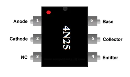
Pinout:
Specifications
| TYPE | DESCRIPTION |
| Category | Isolators Optocouplers, Optoisolators Transistor, Photovoltaic Output Optoisolators |
| Number of Channels | 1 |
| Voltage – Isolation | 5000Vrms |
| Current Transfer Ratio (Min) | 20% @ 10mA |
| Rise / Fall Time (Typ) | 2µs, 2µs |
| Input Type | DC |
| Output Type | Transistor with Base |
| Voltage – Output (Max) | 70V |
| Current – Output / Channel | 50mA |
| Voltage – Forward (Vf) (Typ) | 1.3V |
| Current – DC Forward (If) (Max) | 60 mA |
| Vce Saturation (Max) | 500mV |
| Operating Temperature | -55°C ~ 100°C |
| Mounting Type | Through Hole |
| Package / Case | 6-DIP |
Why to Use 4N25 OPTOCOUPLER
To understand the use of OPTOCOUPLER consider:
Case 1: where you want to isolate LOAD CIRCUIT from CONTROL CIRCUIT. Say you want to control the speed of a small DC motor by using MICROCONTROLLER PWM output. This setup is not feasible as the microcontroller is a sensitive device. So for isolating the load circuit and protecting the controller from voltage fluctuations we use OPTOCOUPLER.
Case 2: Say you want to trigger a MOSFET circuit that is driving a high power load. The MOSFET trigger voltage typically is 12V. These voltage bursts (+12V) needed for the MOSFET driver to control the high power load cannot be drawn from the controller. As controller puts out +3.3V or +5V bursts. In those cases using the 4N25 OPTOCOUPLER chip is ideal.
Case 3: We want to switch a 12V relay which is looping 220V AC fan according to RASPBERRY PI outputs. It is ideal to use 4N25 in this case, as 4N25 draws a negligible amount of power considering a transistor or a MOSFET.
How to Use 4N25 OPTOCOUPLER
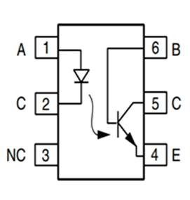
4N25 OPTOCOUPLER IC has two components integrated with it. One is INFRARED DIODE and another of INFRARED PHOTOTRANSISTOR. The IR DIODE is connected between terminals 1 and 2, the PHOTOTRANSISTOR is connected at terminals 4, 5, and 6. The internal setup of the two components can be seen below. The IR radiation emitted by IR LED will not be visible outside the chip. The whole issue of radiation will be working under the background.

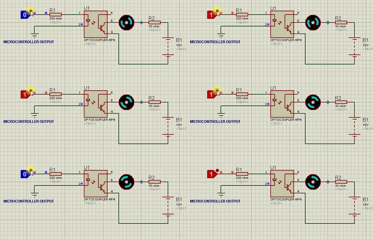
For understanding the OPTOCOUPLER we will consider a circuit shown below.

We will get the +3.3Voltage pulses from a microcontroller and these are driven to the POSITIVE of IR DIODE. When IR DIODE gets powered it will emit Infrared rays internally, when these rays fall on the PHOTOTRANSISTOR the transistor gets turned ON. When the transistor gets turned ON the current flows through the load circuit and the voltage will be seen across the motor. Thus the motor rotates when the microcontroller circuit provides HIGH logic to the 4N25 chip.
When the controller output goes LOW, the IR DIODE input goes LOW. With that, the IR DIODE stops emitting radiation internally. Since radiation is cut off the PHOTOTRANSISTOR gets turned OFF since the radiation acts as BASE TRIGGER. So its a LOW RESISTANCE state to a HIGH RESISTANCE state. With HIGH RESISTANCE the complete supply voltage appears across the transistor and current flow in the load circuit gets ZERO. So the motor stops rotating. Thus the motor stops rotating when the microcontroller input to 4N25 gets LOW.
In this circuit, you can see the motor draws power from the +12V battery source and not from the controller circuit. The PHOTOTRANSISTOR side secondary circuit here is in complete isolation from the CONTROLLER-PHTODIODE primary circuit. The resistors here are placed to limit the currents in the circuit. Make a note the resistance values changed depending on voltages.
Switching Time of 4N25
Under normal circumstances, you have no need to consider the SWITCHING DELAYS of the 4N25 chip. These delays are the response time delays of 4N25. This timing only needs to be considered when switching frequencies goes beyond 1MHz.

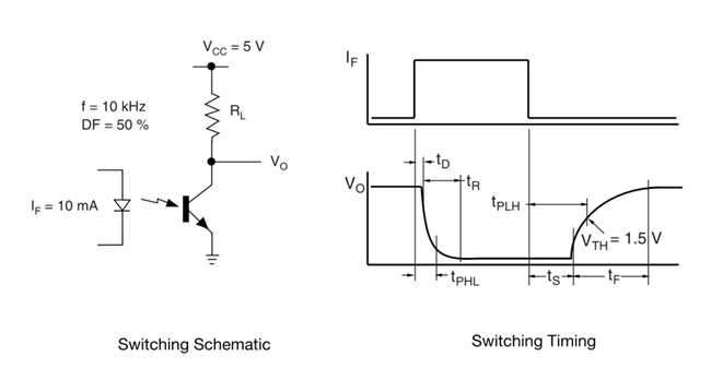
When the switching frequency goes higher, we need to take into account the two parameters of 4N25 in order to avoid errors. These two parameters are RISETIME (tr+td) and FALLTIME (ts+tf). For understanding these parameters consider the circuit above as an example.
In here IF is the IR DIODE forward current. And Vo is the OUTPUT taken. Here Vo goes LOW when the PHOTOTRANSISTOR is ON and Vo goes HIGH when the PHOTOTRANSITOR is OFF. In another sense, it is the voltage across the transistor and it represents the state of the PHOTOTRANSISTOR.
As in the graph, consider the IR DIODE is provided with power, the IR DIODE emits the radiation and the PHOTOTRANSISTOR gets turned ON. But as you can see in the graph, there is a time delay between providing LOGIC INPUT and Vo going LOW at the OUTPUT. This delay in providing a response is called RISETIME (tr+td). The RISETIME (tr+td) of the 4N25 is 2uS.
Similarly, consider the IR DIODE power is cut off, and the PHOTOTRANSISTOR gets turned OFF. But as you can see in the graph there is a time delay between LOGIC INPUT going LOW and Vo going HIGH at the OUTPUT. This delay in providing a response is called FALLTIME (ts+tf). The FALLTIME (ts+tf) of the 4N25 is 2uS.
Here td and ts are in nanosecond so they are usually neglected.
Hence these time delay responses of 4N25 can get stacked leading to major errors. So during high frequencies, one needs to take time delays into consideration.
Applications
- DC motor speed control
- Lighting systems
- PWM applications
- AC mains detection
- Reed relay driving
- Switch mode power supply feedback
- Telephone ring detection
- Logic ground isolation
- Logic coupling with high-frequency noise rejection


