7408 IC Quad 2-Input AND Gates
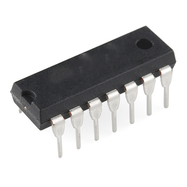
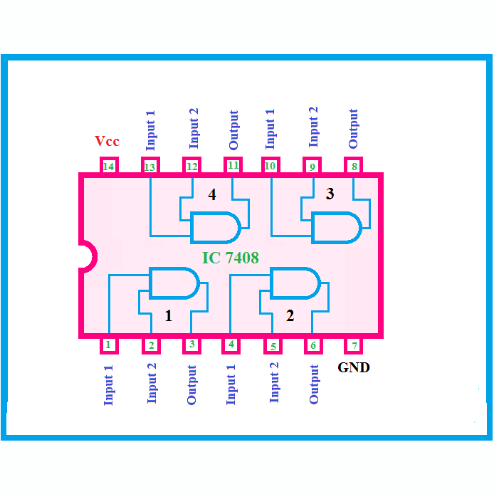
This IC, often found as 74LS08 or 74HC08, is a chip with four basic AND gates. The AND gate is a logic gate – one of the most basic building blocks in digital electronics. The chip comes in a 14-pin package with the following pinout:
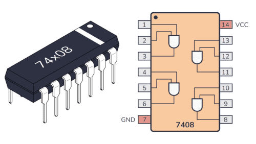
In this guide, you will learn what the 74×08 IC does and how to hook it up in a circuit.
What does the 74C08 / 74LS08 do?
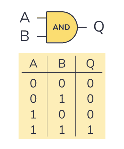
The 74×08 gives you four basic AND gates that can be used individually. An AND gate is a logic gate that outputs 1 (HIGH) only if all of its inputs are 1 (HIGH). In the truth table below, you can see what the output will be for any given input:
How To Use This Chip
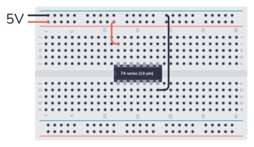
Like every other chip in the 7400 series, this IC needs to be connected to power before you can use it. Most 7400 ICs support a VCC voltage of 5V. One difference between the HC and LS versions of the chip is that the 74HC08 supports 2V to 6V, while the 74LS08 supports only 5V.
Once it’s connected, you can use any of the four basic AND gates inside.
The amount of current you can pull out of each AND gate depends on which chip you are using.
74HC08:
Each output can sink or source 4 mA when powered with 5V.
74LS08:
HIGH-Level Output Current: 0.4 mA
LOW-Level Output Current: 8 mA
74×08 Pinout
The 74×08 has 14 pins and contains four basic AND gates laid out as shown in the pinout diagram below:
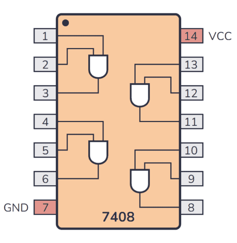
| Pin Name | Pin # | Type | Description |
|---|---|---|---|
| 1A | 1 | Input | Input to the first AND gate. |
| 1B | 2 | Input | Input to the first AND gate. |
| 1Y | 3 | Output | Output from the first AND gate. |
| 2A | 4 | Input | Input to the second AND gate. |
| 2B | 5 | Input | Input to the second AND gate. |
| 2Y | 6 | Output | Output from the second AND gate. |
| GND | 7 | Power | Connect to ground. |
| 3Y | 8 | Output | Output from the third AND gate. |
| 3A | 9 | Input | Input to the third AND gate. |
| 3B | 10 | Input | Input to the third AND gate. |
| 4Y | 11 | Output | Output from the fourth AND gate. |
| 4A | 12 | Input | Input to the fourth AND gate. |
| 4B | 13 | Input | Input to the fourth AND gate. |
| VCC | 14 | Power | Positive power supply. Connect to +5V power. |
Features and Specifications
- Operating voltage range: +4.75 to +5.25V
- Recommended operating voltage: +5V
- Maximum supply voltage:7V
- Maximum current allowed to draw through each gate output: 8mA
- TTL outputs
- Low power consumption
- Typical Rise Time: 18ns
- Typical Fall Time: 18ns
- Operating temperature:0°C to 70°C
- Storage Temperature: -65°C to 150°C
Where to Use 74LS08 IC
There are many applications of IC 74LS08. A few are mentioned below.
1. The chip is basically used where AND logic operation is needed. There are four AND gates in the chip, we can use one or all gates simultaneously.
2. The chip is used in systems where high speed AND operation is needed. As mentioned earlier the gates in the chip are designed by SCHOTTKY TRANSISTORS to make the switching delays of gates less. Because of this the chip can be used for high speed AND operations.
3. 74LS08 is one of the cheapest ICs present in the market for AND logic operation. It is really popular and is available everywhere.
4. The chip provides TTL outputs which are needed in some systems.
Applications
- General purpose ANDlogic operation
- Measuring Instruments
- Digital Electronics
- Servers
- ALUs
- Memory units
- Networking
- Digital systems


