22
h
05
m
17
s
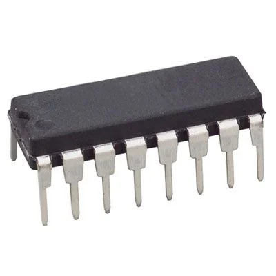
74112 DIP Dual J-K Negative-Edge-Triggered Flip-Flop With Preset and Clear
Original price was: 25.00 EGP.22.00 EGPCurrent price is: 22.00 EGP.
Buy Now

74LS112 Pin Configuration
| Pin No | Pin Name | Description |
|---|---|---|
| 1 | 1CLK | Clock Input 1 |
| 2 | 1K | Input Pin K1 |
| 3 | 1J | Input Pin J1 |
| 4 | 1PRE’ | Active low Preset Pin 1 |
| 5 | 1Q | Output pin Q1 |
| 6 | 1Q’ | Active Low output Pin Q1 |
| 7 | 2Q’ | Active Low output Pin Q2 |
| 8 | GND | Ground Pin |
| 9 | 2Q | Output pin Q2 |
| 10 | 2PRE’ | Active low Preset Pin 2 |
| 11 | 2J | Input Pin J2 |
| 12 | 2K | Input Pin K2 |
| 13 | 2CLK | Clock Input 2 |
| 14 | 2CLR’ | Active low clear/Reset pin 2 |
| 15 | 1CLR’ | Active low clear/Reset pin 1 |
| 16 | Vcc | Chip Supply Voltage |
Features:
- Fully Buffered to Offer Maximum Isolation From External Disturbance
- Package Options Include Plastic Small-Outline (D) Packages, Ceramic Chip Carriers (FK), and Standard Plastic (N) and Ceramic (J) 300-mil DIPs
Specifications:
- Number of Circuits: 2
- Logic Family: LS
- Logic Type: J-K Type Flip-Flop
- Polarity: Inverting/Non-Inverting
- Input Type: TTL
- Output Type: TTL
- High-Level Output Current: -400 uA
- Low-Level Output Current: 8 mA
- Supply Voltage Range: 4.5V ~ 5.5V
- Operating Temperature Range: 0°C ~ 70°C
- Number of Channels: 2
- Number of Input Lines: 5
- Number of Output Lines: 2
- Reset Type: Set, Reset
- Mounting Style: Through Hole
- Package/Case: PDIP-16


Reviews
There are no reviews yet.