7476 IC Dual Master-Slave J-K Flip-Flops
The ‘LS76A contain two independent negative-edge-triggered flip-flops. The J and K inputs must be stable one setup time prior to the high-to-low clock transition for predictable operation. The preset and clear are asynchronous active low inputs. When low they override the clock and data inputs forcing the outputs to the steady state levels as shown in the function table.
the SN74LS76A are characterized for operation from 0°C to 70°C.
Pin Layout

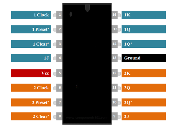
SN74LS76 Pin Configuration
| Pin Number | Pin Name | Description |
| 5 | Vcc | Powers the IC typically with 5V |
| 13 | Ground | Connected to the ground of the system |
| JK Flip Flop – 1 / JK Flip Flop – 2 | ||
| 1,6 | Clock-1/ Clock-2 | These pins must be provided with a clock pulse for the flip-flop |
| 2,7 | Preset-1 / Preset-2 | When the Preset is high the flip flop will set Q=1 and not Q=0 |
| 3, 8 | Clear-1/Clear-2 | When Clear is high the flip flop will set Q=0 and not Q=1 |
| 12,16 | K-1/ K-2 | Input pin of the Flip Flop |
| 4,9 | J-1 / J-2 | Another Input pin of the Flip Flop |
| 10,14 | Q-1(bar) / Q-2 (bar) | The inverted output pin of Flip Flop |
| 11,15 | Q-1 / Q-2 | Output Pin of the Flip Flop |
Features and Specifications
- Dual JK Flip Flop Package IC
- Positive edge triggered Flip-Flop
- Operating Voltage: 4.75V to 5.75V
- Minimum High-Level Input Voltage: 2 V
- Maximum Low-Level Input Voltage: 0.8 V
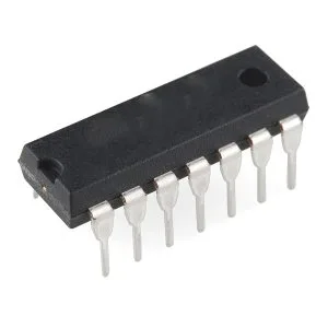
- Available in a 14-pin PDIP package
Applications
- Shift Registers
- Memory/Control Registers
- EEPROM circuits
- Latching devices


