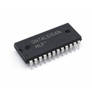



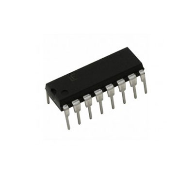
74HC257 Quad 2-input multiplexer IC
Quad 2-input multiplexer with common select and 3-state outputs low-power HC family device (2–6 V), ideal for bus interfacing and data routing.
15.00 EGP
In stockSKU 1794681340805
Buy Now
Shipping across EgyptDelivered to your door
Cash on deliveryPay when your order arrives
Not sure it fits your project?Ask us on WhatsApp - we reply fast
74HC257 IC Quad 2-input multiplexer
The 74HC257 is a high-performance CMOS quad 2-input multiplexer that packages four independent 2-to-1 data selectors plus a common select input and a 3-state output enable. Each section selects between its A and B input pair and presents the selected signal on the corresponding Y output. Built in the ’HC family, the device combines low static power consumption with switching speeds suitable for bus-oriented systems and medium-speed logic.
Designed for bus interfacing and source-selection tasks, the 74HC257’s three-state outputs let multiple devices share a common bus without loading it when output enable (G) is asserted high. The chip accepts standard CMOS input levels across a wide supply range and is pin-compatible with related HC logic, easing substitution and mixed-family designs. Typical use includes routing data lines, selecting between memory or peripheral sources, and simple data-path multiplexing.
Available in PDIP, SOIC, TSSOP and other packages with industry-standard pinouts, the 74HC257 is commonly used where compact, deterministic selection of parallel signals is required. Its low input currents and guaranteed noise margins make it a dependable building block for embedded systems, address/data multiplexing, and multi-source bus architectures.
Features:
- Quad 2-input multiplexers with common select (A/B) and 3-state output enable (G).
- Wide operating supply range: 2 V to 6 V.
- Low power consumption (ICC typically very small; max ≈ 80 µA).
- Typical propagation delay for ’HC257 ≈ 9 ns (fast switching in HC family).
- 3-state outputs allow bus-sharing without loading when disabled.
- Low input current (typical ≤ 1 µA) and good noise margins for robust logic.
Specifications:
| Parameter | Value / Condition |
|---|---|
| Part / Function: | SN74HC257 Quad 2-input multiplexer, 3-state outputs. |
| Recommended VCC (HC): | 2.0 V to 6.0 V. |
| Absolute-maximum VCC: | −0.5 V to +7.0 V. |
| propagation delay (tpd): | ≈ 9 ns See switching tables for VCC dependency. |
| Output drive: | ±6 mA output drive at VCC = 5 V (typical rating). |
| Input current (II): | Typ ≤ 1 µA (VI = VCC or GND). |
| ICC (supply current): | Typ microamps; spec sheet shows up to ≈80 µA (max conditions). |
| I/O tri-state leakage (IOZ): | Specified in datasheet (µA range see electrical table). |
| Input thresholds (VIH / VIL): | VIH / VIL scale with VCC see recommended operating conditions. |
| Operating temperature (TA): | −40 °C to +85 °C (commercial), versions to −55 °C/+125 °C for military CDIP. |
| Package options: | PDIP, SOIC, SOP, TSSOP, CDIP, LCCC |
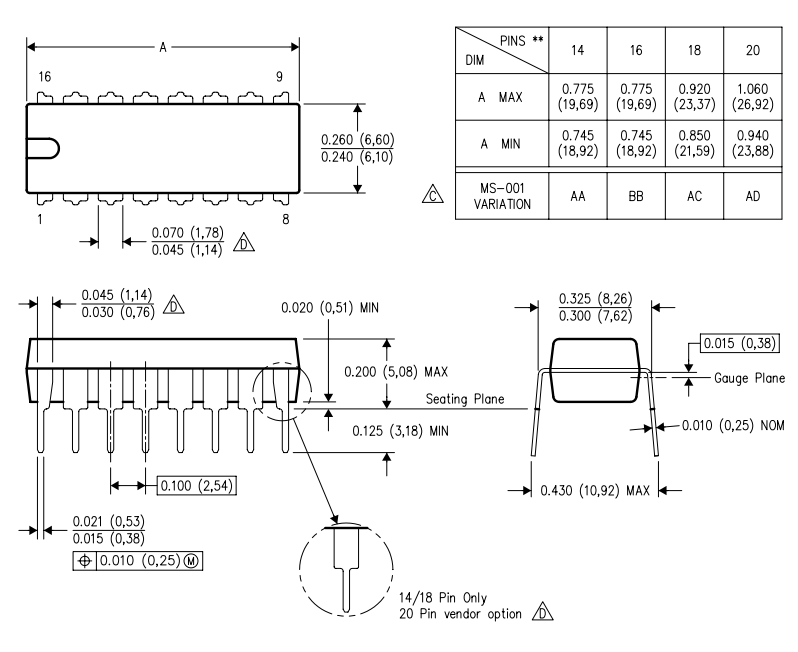
Pinout Diagram:

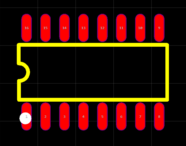
Footprint Diagram:
Applications:
- Bus-oriented systems and multi-source bus interfacing.
- Data path selection and routing in digital systems.
- Address/data multiplexing for memory or peripheral selection.
- Microcontroller / FPGA glue logic for source selection.
Package Contents:
- 1x 74HC257 Quad 2-input multiplexer IC
Datasheet
Related products