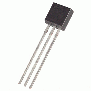
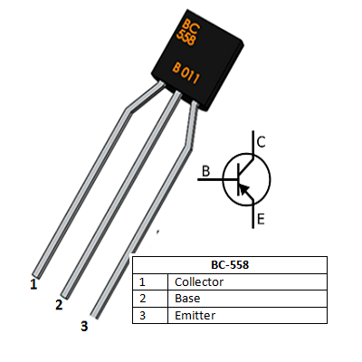
Pinout:
BC558 Transistor Pinout Configuration
| Pin Number | Pin Name | Description |
| 1 | Collector | Current flows in through collector |
| 2 | Base | Controls the biasing of transistor |
| 3 | Emitter | Current Drains out through emitter |
Features
- Bi-Polar PNP Amplifier Transistor
- Collector-Emitter Voltage: -30V
- DC Current Gain (hFE) is 800 maximum
- Collector current (Ic) is -100mA
- Emitter Base Voltage (VBE) is -5V
- Base Current(IB) is -5mA peak
- Available in To-92 Package
Note: Complete technical details can be found in the BC558 datasheet given at the end of this page.
BC558 as switch
When a transistor is used as a switch it is operated in the Saturation and Cut-Off Region as explained above. As discussed a transistor will act as an Open switch during Forward Bias and as a closed switch during Reverse Bias, this biasing can be achieved by supplying the required amount of current to the base pin. A resistor is always added in series with base pin to limit the base current. The value of this resistor (RB) can be calculated using below formulae.
RB = VBE / IB
Where, the value of VBE should be 5V for BC558 and the Base current (IB) depends on the Collector current (IC).
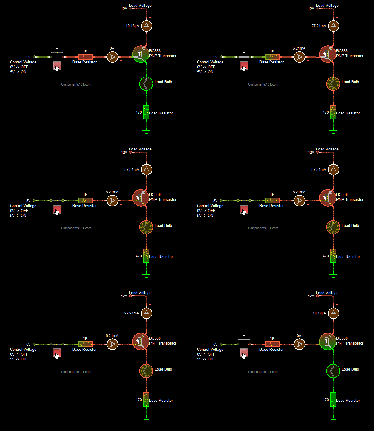
Also note that a PNP transistor is always used for high side switching, meaning the collector is connected to power and emitter to load that is to be switched.
BC558 as Amplifier
A Transistors acts as an Amplifier when operating in Active Region. It can amplify power, voltage and current at different configurations.
Some of the configurations used in amplifier circuits are-
- Common emitter amplifier
- Common collector amplifier
- Common base amplifier
Of the above types, common emitter type (which amplifies voltage) is the popular and mostly used configuration. The BC558 because of this large gain value is normally used to as a audio amplifier. Where an input signal of low voltage is amplified (switched) to high voltages t0 drive loads like speakers. In the below GIF you can notice the transistor being switched for a low voltage (1v) audio signal
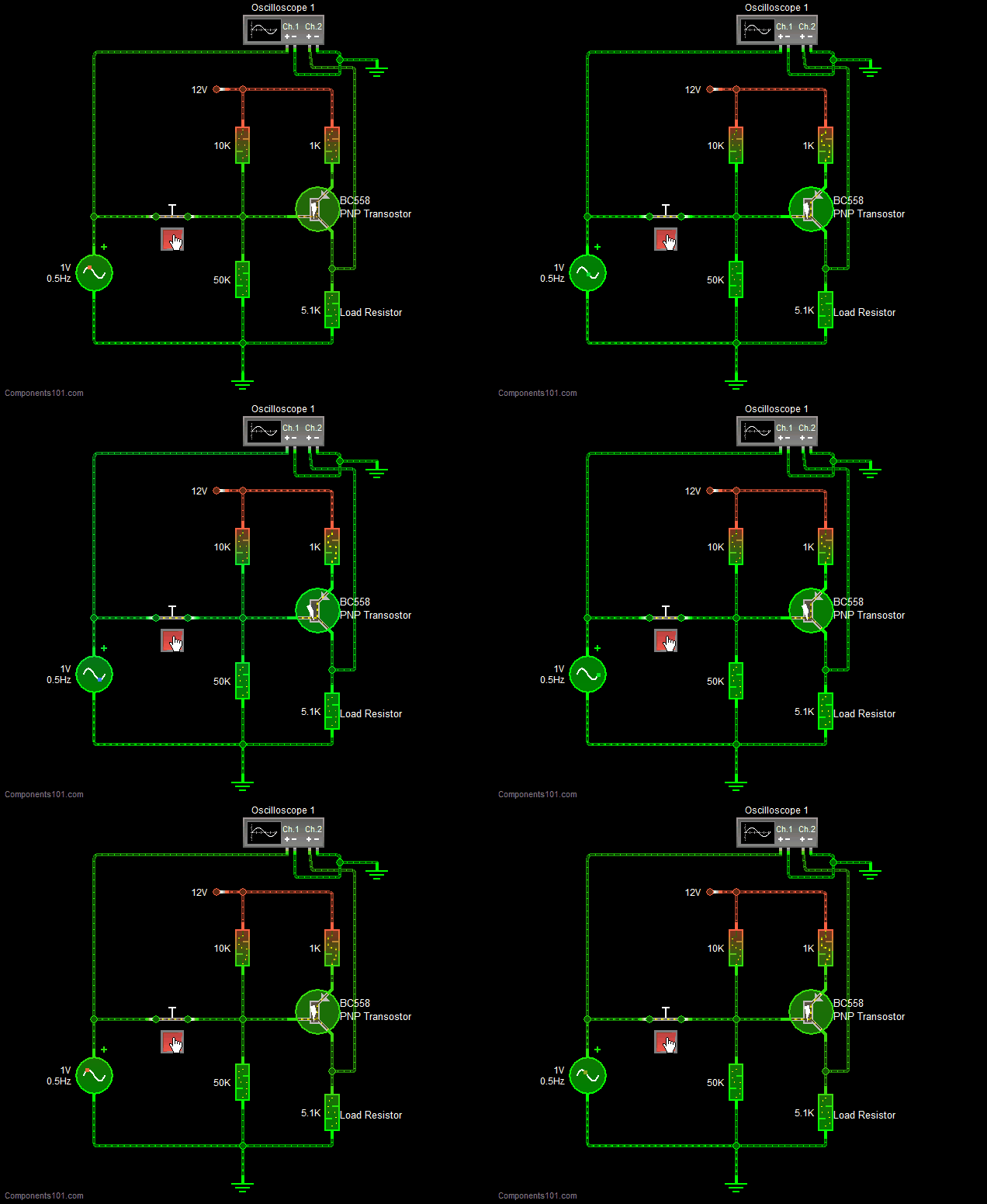
When uses as an Amplifier the DC current gain of the Transistor can be calculated by using the below formulae
DC Current Gain = Collector Current (IC) / Base Current (IB)
Applications
- Build simple audio circuits
- General purpose amplifier
- Driver Modules like Relay Driver, LED driver etc..
- Amplifier modules like Audio amplifiers, signal Amplifier etc..
- Darlington pair


