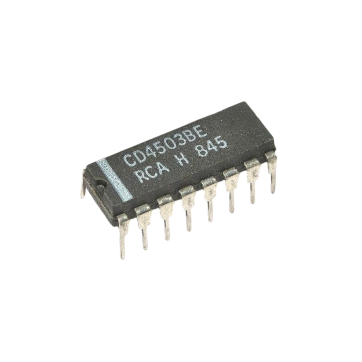
CD4503BE Tri-state Hex Buffer 5V IC DIP-16
The CD4503BE is a CMOS-based hex buffer integrated circuit that contains six independent non-inverting buffer stages. Each output features a tri-state control, allowing it to be placed in a high-impedance state. This makes the IC especially useful in systems where multiple devices share a common data bus, as it helps prevent signal conflicts and ensures proper data flow control.
Designed for reliable operation over a wide voltage range, the CD4503BE offers low power consumption and high noise immunity, making it suitable for various digital logic applications. It is commonly used to interface between different logic families, drive heavier loads, and protect sensitive circuits by isolating stages within a system.
Features:
- Six independent non-inverting buffer channels.
- Tri-state output capability for bus control.
- High noise immunity.
- Low power consumption.
- Wide operating voltage range.
- Suitable for interfacing between logic families.
- High input impedance.
- Output enable control for flexible operation.
Specifications:
| Parameter | Conditions | Min | Typ | Max | Unit |
|---|---|---|---|---|---|
| Supply voltage range (recommended) | TA = full package temperature | 3 | – | 18 | V |
| Quiescent device current | VDD = 5V, TA = 25°C | – | 0.02 | – | µA |
| Quiescent device current | VDD = 15V, TA = 25°C | – | 0.06 | – | µA |
| Output low (sink) current (min) | VDD = 5V, VOL = 0.4V | 2.6 | – | – | mA |
| Output low (sink) current (min) | VDD = 10V, VOL = 0.5V | 9.2 | – | – | mA |
| Output low (sink) current (min) | VDD = 15V, VOL = 1.5V | 19.2 | – | – | mA |
| Output high (source) current (min) | VDD = 5V, VOH = 4.6V | –1.2 | – | – | mA |
| Output high (source) current (min) | VDD = 10V, VOH = 9.5V | –3.1 | – | – | mA |
| Output high (source) current (min) | VDD = 15V, VOH = 13.5V | –8.2 | – | – | mA |
| Input low voltage (VIL) max | VDD = 5V | – | – | 1.5 | V |
| Input high voltage (VIH) min | VDD = 5V | 3.5 | – | – | V |
| Input current (IIN) max | VDD = 18V, TA = 25°C | – | – | ±0.1 | µA |
| Three‑state output leakage | VDD = 18V, TA = 25°C | – | – | ±0.4 | µA |
| Propagation delay time (typical) | CL = 50pF, RL = 200kΩ, VDD = 10V | – | 60 | – | ns |
Pinout:
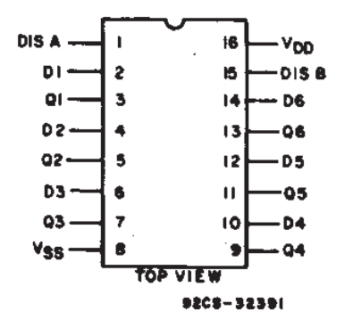
| Pin No. | Pin Name | Description (inferred) |
|---|---|---|
| 1 | DIS A | Disable control for group A (active high) |
| 2 | DI | Data input (likely for channel 1) |
| 3 | QI | Data output (likely for channel 1) |
| 4 | D2 | Possibly channel 2 output (or Q2) |
| 5 | Q2 | Channel 2 output |
| 6 | D3 | Data input for channel 3 |
| 7 | Q3 | Channel 3 output |
| 8 | VSS | Ground (0 V) |
| 9 | Q4 | Channel 4 output |
| 10 | D4 | Data input for channel 4 |
| 11 | Q5 | Channel 5 output |
| 12 | D5 | Data input for channel 5 |
| 13 | Q6 | Channel 6 output |
| 14 | D6 | Data input for channel 6 |
| 15 | DIS B | Disable control for group B (active high) |
| 16 | VDD | Positive supply voltage |
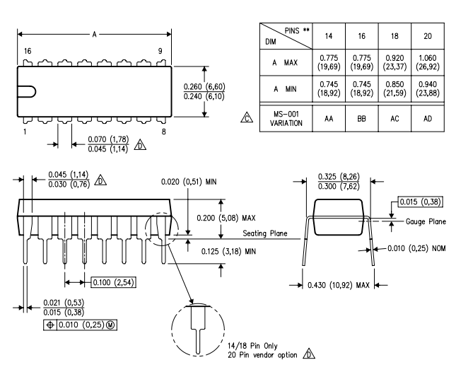
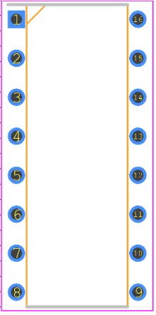
Footprint:
Applications:
- Bus‑oriented microprocessor systems.
- Memory address or data buffering.
- Driving heavily loaded CMOS/TTL lines.
- Three‑state logic interfacing.
- Industrial control and data acquisition.
- LED drivers (with external current limiting).
- General purpose noninverting buffer.
Package Included:
- 1x CD4503BE Tri-state Hex Buffer 5V IC DIP-16.