
ICM7555 General Purpose CMOS Timer DIP
The ICM7555 is a low-power CMOS implementation of the industry-standard 555 timer in a compact DIP-8 package. It is designed to produce accurate time delays and stable oscillations using only a few external components. Compared with bipolar 555 devices, the ICM7555 significantly reduces quiescent current and power-spike behavior during output transitions, making it a better fit for battery-powered and low-power instrumentation.
In operation the chip can be configured as either a monostable (one-shot) or astable (oscillator) timer; a single resistor–capacitor pair controls timing in monostable mode, while two resistors plus a capacitor set frequency and duty cycle in astable mode. The device provides TTL/CMOS-compatible output levels at 5 V and maintains stable timing characteristics across its recommended supply range, simplifying integration into mixed-logic systems.
Mechanically offered in DIP-8, SOP-8, MSOP-8 and DFN-8 packages, the ICM7555 balances compact footprint with straightforward through-hole or surface-mount assembly. Its low leakage on trigger/threshold/reset pins, modest thermal ratings and predictable switching times make it useful for a wide range of control and timing tasks where low standby current and stable timing are important.
Features:
- Very low supply current (typical ~80 µA).
- Steady-state frequency capability up to 500 kHz.
- Wide recommended supply range: 4.5–15 V.
- TTL/CMOS-compatible outputs at 5 V.
- Extremely low trigger/threshold/reset currents (≈20 pA typical).
- Low supply-current spikes during output transitions.
- Pin-compatible with standard 555 timers.
Specifications:
| Specification | Value |
|---|---|
| Recommended supply voltage (VCC): | 4.5 – 15 V. |
| Absolute maximum VCC: | 15 V. |
| Supply current (Is): | VCC=5 V: 30 – 50 µA; VCC=10 V: 60 – 100 µA; VCC=15 V: 90 – 150 µA. |
| Control voltage (VCTRL): | VCC=5 V: 3.28 – 3.38 V (typ 3.33 V). |
| Discharge saturation voltage (VDIS): | VCC=5 V, IDIS=10 mA: 100 – 400 mV. |
| Output low (VOL): | VCC=5 V, IO=3.2 mA: 0.1 – 0.4 V. |
| Output high (VOH): | VCC=5 V, IO=−2 mA: 4.0 – 4.5 V. |
| Trigger voltage (VTRIG): | VCC=5 V: 1.55 – 1.70 V (typ 1.66 V). |
| Trigger current (ITRIG): | VCC=5 V: ≈ 10 pA. |
| Reset voltage (VRES): | VCC=5 V: 0.4 – 1.2 V (typ ≈0.7 V). |
| Reset/threshold leakage currents: | ≈ 10–20 pA (typical). |
| Discharge leakage (IDIS): | VCC=12 V: 1 – 100 nA. |
| Output rise/fall times (tr / tf): | VCC=5 V, RL=10 MΩ, CL=10 pF: typ 35–40 ns, max 75 ns. |
| Maximum steady-state frequency (Fmax): | 500 kHz. |
| Operating temperature (Topr): | −40 to +85 °C. |
| Junction temperature (Tj): | Up to 150 °C. |
| Storage temperature (Tstg): | −50 to +150 °C. |

Pinout Diagram:

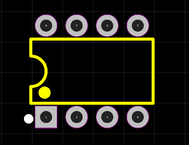
Footprint Diagram:
Applications:
- Pulse generator.
- Precise timing.
- Delay generation.
- Pulse-width modulation (PWM).
Package Contents:
- 1x ICM7555 General Purpose CMOS Timer DIP
Reviews
There are no reviews yet.