PIC16F887-I/P 14KB 2V~5.5V PIC 20MHz 35 PDIP-40 Microcontroller Units (MCUs/MPUs/SOCs)
165.00 EGP
Buy NowPIC16F887 Microcontroller
The PIC16F887 is an 8-bit microcontroller from Microchip. The 40-pin IC has 14 Channel 10-bit ADC making it suitable for applications that require more ADC inputs. The IC also has 2 Comparators, 2 Timers (8-bit and 16-bit) and supports SPI, I2C, and UART communication protocols.
PIC16F887 Microcontroller Overview
The PIC16F887 is an 8-bit microcontroller from Microchip. The 40-pin IC has 14 Channel 10-bit ADC making it suitable for applications that require more ADC inputs. The IC also has 2 Comparators, and 2 Timers (8-bit and 16-bit) and supports SPI, I2C, and UART communication protocols.
It can operate at a speed of up to 20MHz with an external oscillator and also has a precision internal oscillator tunable between 8MHz to 32kHz. The IC supports nanoWatt technology allowing it to consume very low power and operate in Power-Saving sleep mode. It also has a wide operating voltage from 2V to 5.5V making it suitable for battery-powered applications.
The IC also supports safety features like Power-on Reset (POR), Brown-out Reset (BOR), Low Current Watchdog Timer (WDT), etc making it suitable for task-critical and industrial applications. The controller supports In-Circuit Serial Programming (ICSP) allowing the designer to program the controller easily even without removing it from the actual circuit.
Features
| PIC16F887 –Simplified Features | |
| CPU | 8-bit PIC |
| Number of Pins | 40 |
| Operating Voltage (V) | 2 to 5.5 V |
| Number of I/O pins | 35 |
| ADC Module | 14ch, 10-bit |
| Timer Module | 8-bit(2), 16-bit(1) |
| Comparators | 2 |
| DAC Module | Nil |
| Communication Peripherals | UART(1), SPI(1), I2C(1), MSSP(SPI/I2C) |
| External Oscillator | Up to 20Mhz |
| Internal Oscillator | 8Mhz to 32KHz |
| Program Memory Type | Flash |
| Program Memory (KB) | 14KB |
| CPU Speed (MIPS) | 5 MIPS |
| RAM Bytes | 368 |
| Data EEPROM | 256 bytes |
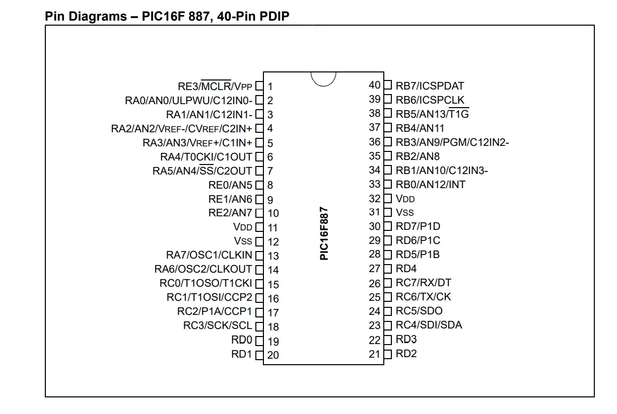
the most pins are multi-functional. For example, designator RA3/AN3/Vref+/C1IN+ for the fifth pin specifies the following functions:
- RA3 Port A third digital input/output
- AN3 Third analog input
- Vref+ Positive voltage reference
- C1IN+ Comparator C1positive input
This small trick is often used because it makes the microcontroller package more compact without affecting its functionality. These various pin functions cannot be used simultaneously but can be changed at any point during operation. The following tables, refer to the PDIP 40 microcontroller.
Pin Description
| Pin Number | Pin Name | Description |
| 1 | MCLR/Vpp/RE3 | MCLR is used during programming, mostly connected to programmer like PicKit or 3rd pin of PORTE |
| 2 | RA0/AN0 | Analog pin 0 or 0th pin of PORTA |
| 3 | RA1/AN1 | Analog pin 1 or 1st pin of PORTA |
| 4 | RA2/AN2/Vref- | Analog pin 2 or 2nd pin of PORTA |
| 5 | RA3/AN3/Vref+ | Analog pin 3 or 3rd pin of PORTA |
| 6 | RA4/T0CKI/C1out | 4th pin of PORTA |
| 7 | RA5/AN4/SS/C2out | Analog pin 4 or 5th pin of PORTA |
| 8 | RE0/RD/AN5 | Analog pin 5 or 0th pin of PORTE |
| 9 | RE1/WR/AN6 | Analog pin 6 or 1st pin of PORTE |
| 10 | RE2/CS/AN7 | Analog pin 6 or 2nd pin of PORTE |
| 11 | Vdd | Ground pin of MCU |
| 12 | Vss | Positive pin of MCU (+5V) |
| 13 | RA7/OSC1/CLKI | External Oscillator/clock input pin or 7th pin of PORTA |
| 14 | RA6/OSC2/CLKO | External Oscillator/clock output pin or 6th pin of PORTA |
| 15 | RC0/T1OSO/T1CKI | 0th pin of PORT C |
| 16 | RC1/T1OSI/CCP2 | 1st pin of POCTC or Timer/PWM pin |
| 17 | RC2/CCP1 | 2nd pin of POCTC or Timer/PWM pin |
| 18 | RC3/SCK/SCL | 3rd pin of POCTC |
| 19 | RD0 | 0th pin of POCTD |
| 20 | RD1 | 1st pin of POCTD |
| 21 | RD2 | 2nd pin of POCTD |
| 22 | RD3 | 3rd pin of POCTD |
| 23 | RC4/SDI/SDA | 4th pin of POCTC or Serial Data in pin |
| 24 | RC5/SDO | 5th pin of POCTC or Serial Data Out pin |
| 25 | RC6/Tx/CK | 6th pin of POCTC or Transmitter pin of Microcontroller |
| 26 | RC7/Rx/DT | 7th pin of POCTC or Receiver pin of Microcontroller |
| 27 | RD4 | 4th pin of POCTD |
| 28 | RD5/P1B | 5th pin of POCTD |
| 29 | RD6/P1C | 6th pin of POCTD |
| 30 | RD7/P1D | 7th pin of POCTD |
| 31 | Vss | Positive pin of MCU (+5V) |
| 32 | Vdd | Ground pin of MCU |
| 33 | RB0/INT | 0th pin of POCTB or External Interrupt pin |
| 34 | RB1/AN10 | Analog pin 10 or 1st pin of POCTB |
| 35 | RB2 /AN8 | Analog pin 8 or 2nd pin of POCTB |
| 36 | RB3/PGM/AN9 | Analog pin 9 or 3rd pin of POCTB or connected to programmer |
| 37 | RB4/AN11 | Analog pin 11 or 4th pin of POCTB |
| 38 | RB5/AN13 | Analog pin 13 or 5th pin of POCTB |
| 39 | RB6/PGC | 6th pin of POCTB or connected to programmer |
| 40 | RB7/PGD | 7th pin of POCTB or connected to programmer |
Applications
- Design requiring many ADC channels
- Battery Operated Low Power applications
- Design requiring Multiple I/O interfaces and communications
- Ideal for more advanced level A/D applications in automotive, industrial, appliances, and consumer applications.



Reviews
There are no reviews yet.