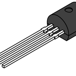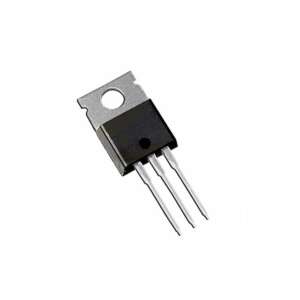





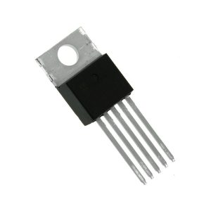


STP75NF75 N-Channel MOSFET Transistor 75V 9.5mΩ 80A TO-220
STP75NF75: N-channel 75V, 80A, 0.0095Ω STripFET™ II Power MOSFET. Designed for minimal gate charge in high-efficiency switching applications.
35.00 EGP
In stockSKU 3496300095988
Buy Now
Shipping across EgyptDelivered to your door
Cash on deliveryPay when your order arrives
Not sure it fits your project?Ask us on WhatsApp - we reply fast
STP75NF75 N-Channel MOSFET Transistor 75V 9.5mΩ 80A TO-220
The STP75NF75 is an N-channel 75V, 80A Power MOSFET from STMicroelectronics. It is built using the unique STripFET™ II process, which is specifically designed to minimize input capacitance and gate charge.
This design makes it an excellent choice as the primary switch in advanced high-efficiency, high-frequency isolated DC-DC converters, particularly for Telecom and Computer applications. It is also well-suited for any application that requires low gate drive power.
Features
- Technology: STripFET™ II Power MOSFET
- Low On-Resistance
- Low Gate Charge
- High dv/dt
- Robustness: 100% avalanche tested
Specifications
| Parameter | Symbol | Value | Conditions / Notes |
|---|---|---|---|
| General Characteristics | |||
| Drain-Source Voltage | VDS | 75 V | |
| Continuous Drain Current | ID | 80 A | at TC=25°C |
| Static Drain-Source On-Resistance (Max) | RDS(on) | 0.0095 Ω | at VGS=10V, ID=40A |
| Absolute Maximum Ratings (at TC=25°C) | |||
| Drain-Source Voltage (VGS=0) | VDS | 75 V | |
| Gate-Source Voltage | VGS | ±20 V | |
| Continuous Drain Current | ID | 80 A | at TC=25°C |
| Continuous Drain Current | ID | 70 A | at TC=100°C |
| Pulsed Drain Current | IDM | 320 A | Pulse width limited by SOA |
| Total Power Dissipation | PTOT | 300 W | at TC=25°C |
| Operating Junction Temperature | TJ | -55 to 175 °C | |
| Single Pulse Avalanche Energy | EAS | 700 mJ | Starting TJ=25°C, ID=40A, VDD=37.5V |
| Thermal Data | |||
| Thermal Resistance Junction-Case (Max) | RthJC | 0.5 °C/W | Applies to TO-220 package |
| Thermal Resistance Junction-Ambient (Max) | RthJA | 62.5 °C/W | Applies to TO-220 package |
| Electrical Characteristics (at TC=25°C unless noted) | |||
| Gate Threshold Voltage | VGS(th) | 2V (Min), 3V (Typ), 4V (Max) | VDS=VGS, ID=250μA |
| Total Gate Charge | Qg | 117 nC (Typ), 160 nC (Max) | VDD=60V, ID=80A, VGS=10V |
| Input Capacitance | Ciss | 3700 pF (Typ) | VDS=25V, f = 1 MHz, VGS=0 |
| Output Capacitance | Coss | 730 pF (Typ) | |
| Reverse Transfer Capacitance | Crss | 240 pF (Typ) | |
| Switching Times (Typical values) | |||
| Turn-on Delay Time | td(on) | 25 ns | VDD=37.5V, ID=45A, RG=4.7Ω, VGS=10V |
| Rise Time | tr | 100 ns | |
| Turn-off Delay Time | td(off) | 66 ns | |
| Fall Time | tf | 30 ns | |

Applications
- General high-frequency switching applications
- Primary switch in high-efficiency DC-DC converters
- Telecom and computer power supplies
- Any application requiring low gate drive power
DataSheet
Related products