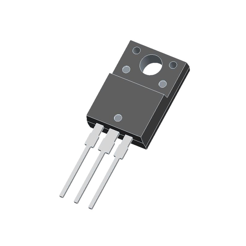
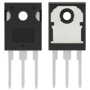
TOSHIBA 2SK2700 N-Channel MOSFET Transistor 900V 3A 2-10R1B
The 2SK2700 is a Silicon N-Channel MOSFET Type (π–MOSIII) Field Effect Transistor manufactured by TOSHIBA. Operating in enhancement mode, this component is engineered to provide high forward transfer admittance while maintaining low leakage current.
Features
- Low Drain-Source ON Resistance: RDS (ON) = 3.7 Ω (typ.)
- High Forward Transfer Admittance: |Yfs| = 2.6 S (typ.)
- Low Leakage Current: IDSS = 100 μA (max) (VDS = 720 V)
- Enhancement Operation: Vth = 2.0 to 4.0 V (VDS = 10 V, ID = 1 mA)
Specifications
Absolute Maximum Ratings (Ta = 25°C)
| Characteristics |
Symbol |
Rating |
Unit |
| Drain-source voltage |
VDSS |
900 |
V |
| Drain-gate voltage (RGS = 20 kΩ) |
VDGR |
900 |
V |
| Gate-source voltage |
VGSS |
±30 |
V |
| Drain current (DC) |
ID |
3 |
A |
| Drain current (Pulse) |
IDP |
9 |
A |
| Drain power dissipation (Tc = 25°C) |
PD |
40 |
W |
| Single pulse avalanche energy |
EAS |
295 |
mJ |
| Avalanche current |
IAR |
3 |
A |
| Repetitive avalanche energy |
EAR |
4 |
mJ |
| Channel temperature |
Tch |
150 |
°C |
| Storage temperature range |
Tstg |
-55 to 150 |
°C |
Thermal Characteristics
| Characteristics |
Symbol |
Max |
Unit |
| Thermal resistance, channel to case |
Rth (ch-c) |
3.125 |
°C/W |
| Thermal resistance, channel to ambient |
Rth (ch-a) |
62.5 |
°C/W |
Electrical Characteristics (Ta = 25°C)
| Characteristics |
Symbol |
Test Condition |
Min |
Typ. |
Max |
Unit |
| Gate leakage current |
IGSS |
VGS = ±30 V, VDS = 0 V |
— |
— |
±10 |
μA |
| Gate-source breakdown voltage |
V(BR)GSS |
IG = ±10 μA, VDS = 0 V |
+30 |
— |
— |
V |
| Drain cut-off current |
IDSS |
VDS = 720 V, VGS = 0 V |
— |
— |
100 |
μA |
| Drain-source breakdown voltage |
V(BR)DSS |
ID = 10 mA, VGS = 0 V |
900 |
— |
— |
V |
| Gate threshold voltage |
Vth |
VDS = 10 V, ID = 1 mA |
2.0 |
— |
4.0 |
V |
| Drain-source ON resistance |
RDS (ON) |
VGS = 10 V, ID = 1.5 A |
— |
3.7 |
4.3 |
Ω |
| Forward transfer admittance |
|Yfs| |
VDS = 20 V, ID = 1.5 A |
0.65 |
2.6 |
— |
S |
| Input capacitance |
Ciss |
VDS = 25 V, VGS = 0 V, f = 1 MHz |
— |
750 |
— |
pF |
| Reverse transfer capacitance |
Crss |
— |
10 |
— |
pF |
| Output capacitance |
Coss |
— |
70 |
— |
pF |
| Rise time |
tr |
VDD ≈ 200 V, ID = 1.5 A, VGS = 10 V, Vout, RL = 133 Ω, RG = 50 Ω, Duty ≤ 1%, tw = 10 μs |
— |
15 |
— |
ns |
| Turn-on time |
ton |
— |
55 |
— |
ns |
| Fall time |
tf |
— |
30 |
— |
ns |
| Turn-off time |
toff |
— |
110 |
— |
ns |
| Total gate charge (gate-source plus gate-drain) |
Qg |
VDD ≈ 400 V, VGS = 10 V, ID = 3 A |
— |
25 |
— |
nC |
| Gate-source charge |
Qgs |
— |
13 |
— |
nC |
| Gate-drain (“miller”) charge |
Qgd |
— |
12 |
— |
nC |
Source-Drain Ratings and Characteristics (Ta = 25°C)
| Characteristics |
Symbol |
Test Condition |
Min |
Typ. |
Max |
Unit |
| Continuous drain reverse current |
IDR |
— |
— |
— |
3 |
A |
| Pulse drain reverse current |
IDRP |
— |
— |
— |
9 |
A |
| Forward voltage (diode) |
VDSF |
IDR = 3 A, VGS = 0 V |
— |
— |
-1.9 |
V |
| Reverse recovery time |
trr |
IDR = 3 A, VGS = 0 V, dIDR/dt = 100 A/μs |
— |
1100 |
— |
ns |
| Reverse recovery charge |
Qrr |
— |
7.2 |
— |
μC |

Applications
- Chopper Regulators
- DC-DC Converters
- Motor Drive Applications
Package Content
- 1 x TOSHIBA 2SK2700 N-Channel MOSFET Transistor 900V 3A 2-10R1B
DataSheet