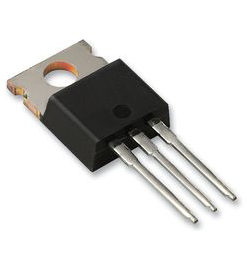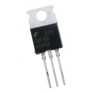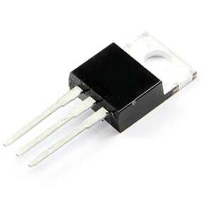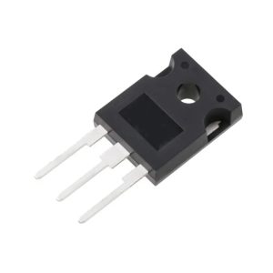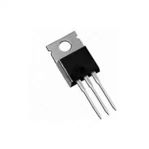







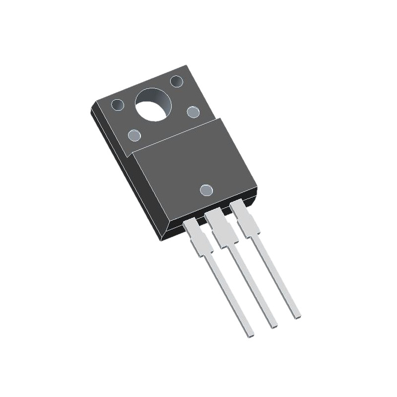
2SK2632 N-Channel MOSFET Transistor 800V 2.5A TO-220F
N-Channel MOSFET, 800V, 2.5A, TO-220F package. Ultrahigh-speed switching with low ON-resistance and low gate charge.
15.00 ج.م
متوفرالكود 3496300160686
اشترِ الآن
شحن لجميع محافظات مصريصلك حتى باب بيتك
الدفع عند الاستلامادفع عند وصول طلبك
غير متأكد أنه يناسب مشروعك؟اسألنا على واتساب - نرد بسرعة
2SK2632 N-Channel MOSFET Transistor 800V 2.5A TO-220F
The 2SK2632 is an N-channel silicon MOSFET designed for ultrahigh-speed switching applications. It blocks a minimum of 800V between drain and source and carries a continuous DC drain current of 2.5A (7.5A pulsed). Its two headline characteristics — low ON-resistance (RDS(on) = 3.6Ω typ. / 4.8Ω max. at VGS = 15V) and low total gate charge (Qg = 15nC typ.) — give it true nanosecond-class switching speed, with typical turn-ON delay and rise times of 15ns and turn-OFF delay and fall times of 45ns and 23ns respectively.
Features
- N-channel silicon MOSFET for ultrahigh-speed switching applications
- 800V minimum drain-to-source breakdown voltage
- 2.5A continuous (DC) drain current; 7.5A pulsed (PW ≤ 10µs, duty cycle ≤ 1%)
- Low ON-resistance: RDS(on) = 3.6Ω typ. / 4.8Ω max. (VGS = 15V, ID = 1.3A)
- Low total gate charge: Qg = 15nC typ. (VDS = 200V, VGS = 10V, ID = 2.5A)
- Very fast switching: td(on) = 15ns, tr = 15ns, td(off) = 45ns, tf = 23ns (typ.)
- Low capacitances: Ciss = 550pF, Coss = 150pF, Crss = 70pF (typ. at VDS = 20V, f = 1MHz)
- Very low leakage: IDSS ≤ 1.0µA (VDS = 800V); IGSS ≤ ±100nA (VGS = ±30V)
- Gate cutoff voltage 3.5V–5.5V; gate rating ±30V
- Built-in body diode: VSD = 0.84V typ. / 1.2V max. (IS = 2.5A)
- Power dissipation 2.0W (Ta = 25°C) / 25W (Tc = 25°C); channel temperature up to 150°C
- 3-pin TO-220FI-LS package; marking K2632
Specifications
Absolute Maximum Ratings (Ta = 25°C)
| Parameter | Symbol | Conditions | Rating | Unit |
|---|---|---|---|---|
| Drain-to-Source Voltage | VDSS | — | 800 | V |
| Gate-to-Source Voltage | VGSS | — | ±30 | V |
| Drain Current (DC) | ID | — | 2.5 | A |
| Drain Current (Pulse) | IDP | PW ≤ 10 µs, duty cycle ≤ 1% | 7.5 | A |
| Allowable Power Dissipation | PD | Ta = 25°C | 2.0 | W |
| Allowable Power Dissipation | PD | Tc = 25°C | 25 | W |
| Channel Temperature | Tch | — | 150 | °C |
| Storage Temperature | Tstg | — | –55 to +150 | °C |
Electrical Characteristics (Ta = 25°C)
| Parameter | Symbol | Test Conditions | Min | Typ | Max | Unit |
|---|---|---|---|---|---|---|
| Drain-to-Source Breakdown Voltage | V(BR)DSS | VGS = 0 V, ID = 1 mA | 800 | – | – | V |
| Zero Gate-Voltage Drain Current | IDSS | VGS = 0 V, VDS = 800 V | – | – | 1.0 | µA |
| Gate-to-Source Leakage Current | IGSS | VDS = 0 V, VGS = ±30 V | – | – | ±100 | nA |
| Cutoff Voltage | VGS(off) | VDS = 10 V, ID = 1 mA | 3.5 | – | 5.5 | V |
| Forward Transfer Admittance | |yfs| | VDS = 10 V, ID = 1.3 A | 0.7 | 1.4 | – | S |
| Static Drain-to-Source On-State Resistance | RDS(on) | VGS = 15 V, ID = 1.3 A | – | 3.6 | 4.8 | Ω |
| Input Capacitance | Ciss | VDS = 20 V, f = 1 MHz | – | 550 | – | pF |
| Output Capacitance | Coss | VDS = 20 V, f = 1 MHz | – | 150 | – | pF |
| Reverse Transfer Capacitance | Crss | VDS = 20 V, f = 1 MHz | – | 70 | – | pF |
| Total Gate Charge | Qg | VDS = 200 V, VGS = 10 V, ID = 2.5 A | – | 15 | – | nC |
| Turn-ON Delay Time | td(on) | Specified test circuit* | – | 15 | – | ns |
| Rise Time | tr | Specified test circuit* | – | 15 | – | ns |
| Turn-OFF Delay Time | td(off) | Specified test circuit* | – | 45 | – | ns |
| Fall Time | tf | Specified test circuit* | – | 23 | – | ns |
| Diode Forward Voltage | VSD | VGS = 0 V, IS = 2.5 A | – | 0.84 | 1.2 | V |

Applications
- Ultrahigh-speed / high-voltage switching circuits
- Fast switching power stages where low gate-charge drive and low ON-resistance losses are needed
- General high-voltage N-channel switch replacement
Package Content
- 1 x 2SK2632 N-Channel MOSFET Transistor 800V 2.5A TO-220F
DataSheet
منتجات ذات صلة