-
-

-
-

AC-04 Wireless Trigger System with 4 Channel Transceiver with 3.5mm to 6.35mm Adapter
900.00 ج.م900.00 ج.م×
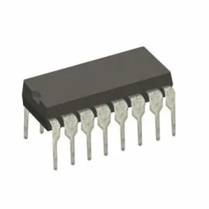

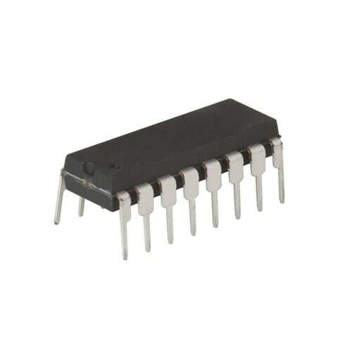
CD4043 IC Quad NOR R/S Latch with 3-State Outputs
CD4043 High-performance CMOS quad NOR R/S latch IC with 3-state outputs for flexible digital logic design.
22.00 ج.م
متوفرالكود 8151487934721
اشترِ الآن
شحن لجميع محافظات مصريصلك حتى باب بيتك
الدفع عند الاستلامادفع عند وصول طلبك
غير متأكد أنه يناسب مشروعك؟اسألنا على واتساب - نرد بسرعة
CD4043 IC Quad NOR R/S Latch with 3-State Outputs
The CD4043 IC is a CMOS quad cross-coupled NOR R/S latch with 3-state outputs. It contains four independently controlled latches, each providing separate SET and RESET inputs along with a dedicated Q output. A common ENABLE input allows simultaneous control of all latch outputs, supporting direct bus interface without the need for additional components.
Features:
- Wide supply voltage range: 3V to 15V
- Low power: 100 nW (typ.)
- High noise immunity: 0.45 VDD (typ.)
- Separate SET and RESET inputs for each latch
- NOR and NAND configuration
- 3-STATE output with common output enable
Specifications:
- Supply Voltage: 3 ~ 15V
- Supply Current: 40 nA
- Product Category: Latches
- Number of Circuits: 1 Circuit
- Type: S-R Type
- Number of Channels: 4 Channels
- Number of Input Lines: 8 Line
- Output Type: 3-State
- Product Type: Latches
- Reset Type: No Reset
- Polarity: Non-Inverting
- Quiescent Current: 20 uA
- Number of Output Lines: 4 Line
- High Level Output Current: -4.2 mA
- Low Level Output Current: 32 mA
- Propagation Delay Time: 300 ns at 5V, 140 ns at 10V, 100 ns at 15V
- Logic Type: CMOS Quad NOR S/R Latch with 3-State Output
- Minimum Operating Temperature: -55 ~ +125°C
- Mounting Style: Through Hole
- Package/Case: PDIP-16
CD4043 Pinout
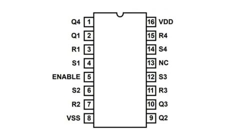
| Pin No | Pin Name | Description |
|---|---|---|
| 1 | Q4 | output of latch 4 |
| 2 | Q1 | output of latch 1 |
| 3 | R1 | reset input latch 1 |
| 4 | S1 | set input latch 1 |
| 5 | ENB | enable pin |
| 6 | S2 | set input latch 2 |
| 7 | R2 | reset input latch 2 |
| 8 | VSS | source supply |
| 9 | Q2 | output of latch 2 |
| 10 | Q3 | output of latch 3 |
| 11 | R3 | reset input latch 3 |
| 12 | S3 | set input latch 3 |
| 13 | NC | no connection |
| 14 | S4 | set input latch 4 |
| 15 | R4 | reset input latch 4 |
| 16 | VDD | Drain supply |
Applications:
- Temporary data storage elements.
- Multiple bus storage systems.
- Strobed register designs.
- Four-bit independent latch circuits with enable control.
- General digital logic and timing applications.
Datasheet:
منتجات ذات صلة