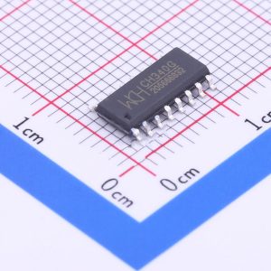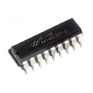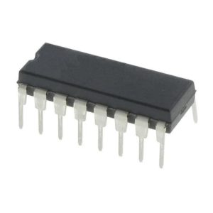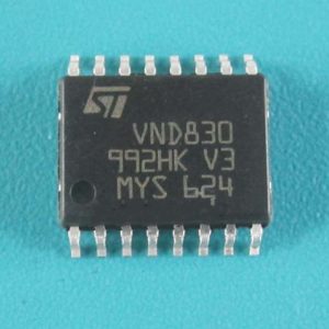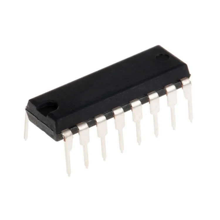
HD14530BP CMOS Integrated Circuit IC DIP-16
The HD14530BP is a dual five-input majority logic gate implemented in CMOS. Each gate evaluates five logic inputs (A–E) plus a control/test input W; the output Z is driven high when three or more inputs are logical “1.” The device’s monolithic CMOS structure uses P- and N-channel enhancement transistors and includes diode protection on every input. It accepts a wide supply range and can directly drive standard TTL loads.
Functionally the HD14530BP simplifies many combinational and sequential circuits by providing majority-logic primitives (5-input and 3-input majority behavior) that can be reconfigured by tying inputs or using W as a control to realize OR, AND, NAND, NOR, XNOR and related functions with fewer external parts. The device incorporates static-protection circuitry to reduce ESD risk; the datasheet notes unused inputs must be tied to VSS or VDD.
The datasheet covers plastic DIP-16, ceramic DIP and SOIC packages with full pin assignments (VDD = pin 16, VSS = pin 8) and outline drawings. Electrical data include input thresholds, VOH/VOL, drive currents, quiescent and dynamic supply currents, input capacitance, and timing (propagation delays and rise/fall times) at VDD = 5, 10 and 15 V. Example circuits shown include flip-flops and astable multivibrators.
Features:
- Diode protection on all inputs.
- Wide operating supply range: 3.0 V to 18 V.
- Dual five-input majority logic gates (A–E inputs plus W control).
- Capable of driving two low-power TTL loads or one low-power Schottky-TTL load.
- Built-in static-protection circuitry (ESD protection).
- Unused inputs must be tied to a defined logic level (VSS or VDD).
Specifications:
| Parameter | Value / Notes (from datasheet) |
|---|---|
| Recommended operating supply: | 3.0 V to 18 V |
| Maximum DC supply rating (VDD): | –0.5 V to +18.0 V (maximum rating) |
| Input / output voltage range: | –0.5 V to VDD + 0.5 V (DC or transient) |
| Input / output current (per pin): | ±10 mA (max) |
| Power dissipation (per package): | 500 mW (max) |
| Input capacitance (Cin): | 5.0 pF, Max 7.5 pF |
| Quiescent current (IDD, per package): | ~0.25 µA (5 V) increases with VDD (see datasheet table) |
| Output drive (typical at VDD = 5 V): | IOH ≈ –3.0 mA (source) IOL ≈ 0.64 mA (sink) (see electrical table for other VDD) |
| Propagation delay (typ, examples at 5 V, CL=50 pF): | tPLH ≈ 375 ns tPHL ≈ 430 ns (see switching table for detailed formulas and VDD = 10/15 V values) |

Pinout:

Applications:
- Sequential Logic Circuit.
- Majority-Logic Control Module.
- Custom Flip-Flop Logic.
- Multivibrator Circuit.
- Digital Logic Processing Unit.
Package Contents:
- 1x HD14530BP Integrated Circuit IC DIP-16