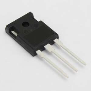




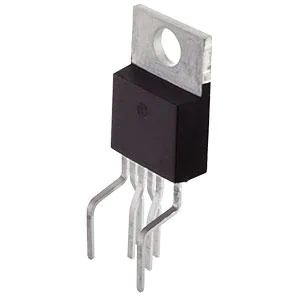



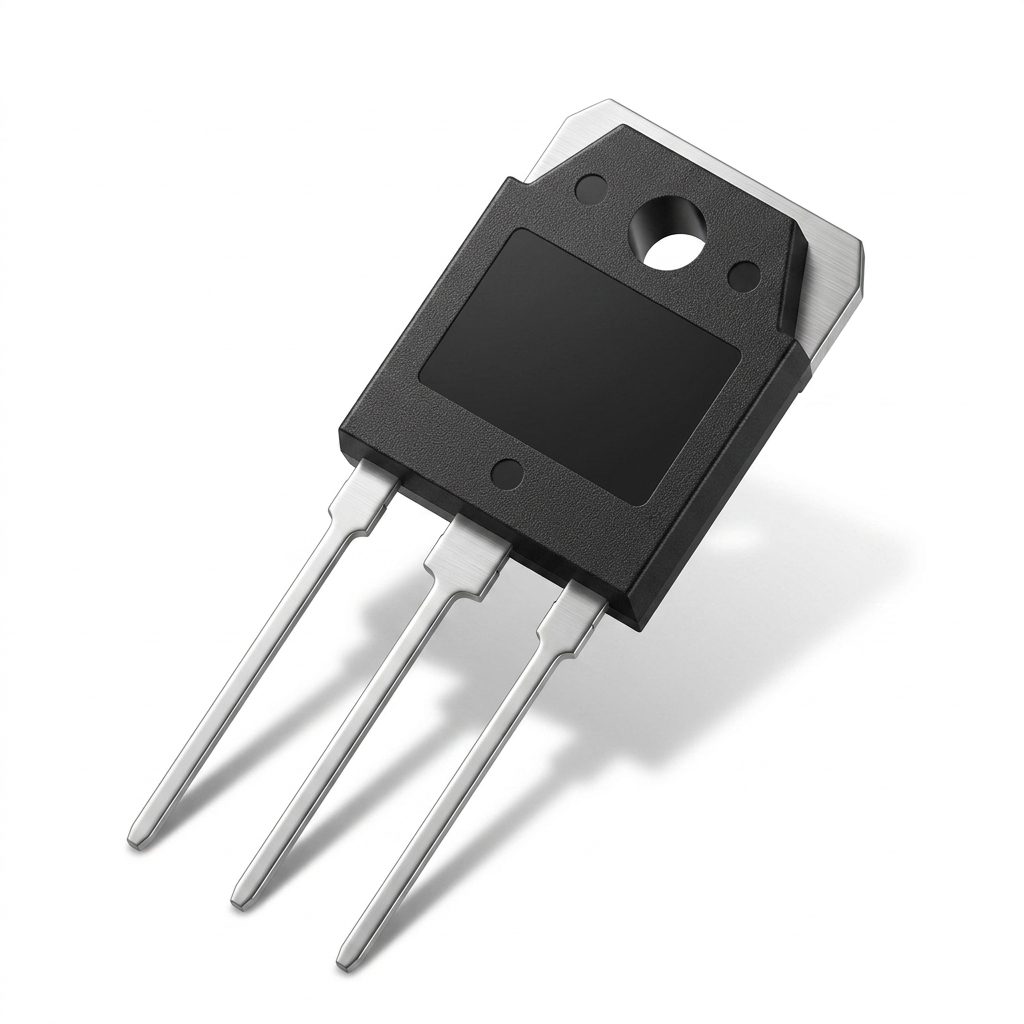
Silan 23N50 N-Channel Power MOSFET 500V 23A TO-3P
Silan 23N50: 500V, 23A N-Channel Power MOSFET in TO-3P. Low RDS(on) 0.21Ω, fast switching for AC-DC/DC-DC converters & PWM motor drivers.
85.00 EGP
In stockSKU 3496300159468
Buy Now
Shipping across EgyptDelivered to your door
Cash on deliveryPay when your order arrives
Not sure it fits your project?Ask us on WhatsApp - we reply fast
Silan 23N50 N-Channel Power MOSFET 500V 23A TO-3P
The 23N50 is a 23A, 500V N-channel enhancement-mode power MOS field effect transistor produced by Silan Microelectronics using Silan’s proprietary F-Cell™ structure VDMOS technology.
The improved planar stripe cell and improved guard ring terminal have been especially tailored to minimize on-state resistance, provide superior switching performance, and withstand high energy pulses in the avalanche and commutation modes.
Features
- 23A, 500V, RDS(on) (typ.) = 0.21Ω @ VGS = 10V
- Low gate charge (Qg = 42.51nC typ.)
- Low Crss (10.1pF typ.)
- Fast switching (td(on) = 42.2ns, tf = 71.2ns typ.)
- Improved dv/dt capability
- High single-pulse avalanche energy: EAS = 2044mJ
- Operating junction temperature range: −55°C to +150°C
Specifications
| Characteristic | Symbol | Test Conditions | Min. | Typ. | Max. | Unit |
|---|---|---|---|---|---|---|
| ABSOLUTE MAXIMUM RATINGS (TC = 25°C unless otherwise noted) | ||||||
| Drain-Source Voltage | VDS | – | – | – | 500 | V |
| Gate-Source Voltage | VGS | – | – | – | ±30 | V |
| Drain Current (TC = 25°C) | ID | – | – | – | 23.0 | A |
| Drain Current (TC = 100°C) | ID | – | – | – | 14.55 | A |
| Drain Current – Pulsed | IDM | – | – | – | 92.0 | A |
| Power Dissipation (TC = 25°C) | PD | – | – | – | 280 | W |
| Power Dissipation – Derate above 25°C | PD | – | – | – | 2.24 | W/°C |
| Single Pulsed Avalanche Energy (Note 1) | EAS | – | – | – | 2044 | mJ |
| Operating Junction Temperature Range | TJ | – | -55 | – | +150 | °C |
| Storage Temperature Range | Tstg | – | -55 | – | +150 | °C |
| THERMAL CHARACTERISTICS | ||||||
| Thermal Resistance, Junction-to-Case | RθJC | – | – | 0.45 | – | °C/W |
| Thermal Resistance, Junction-to-Ambient | RθJA | – | – | 50 | – | °C/W |
| ELECTRICAL CHARACTERISTICS (TC = 25°C unless otherwise noted) | ||||||
| Drain-Source Breakdown Voltage | BVDSS | VGS = 0V, ID = 250µA | 500 | – | – | V |
| Drain-Source Leakage Current | IDSS | VDS = 500V, VGS = 0V | – | – | 1.0 | µA |
| Gate-Source Leakage Current | IGSS | VGS = ±30V, VDS = 0V | – | – | ±100 | nA |
| Gate Threshold Voltage | VGS(th) | VGS = VDS, ID = 250µA | 2.0 | – | 4.0 | V |
| Static Drain-Source On-State Resistance | RDS(on) | VGS = 10V, ID = 11.5A | – | 0.21 | 0.27 | Ω |
| Input Capacitance | Ciss | VDS = 25V, VGS = 0V, f = 1.0MHz | – | 2595.8 | – | pF |
| Output Capacitance | Coss | VDS = 25V, VGS = 0V, f = 1.0MHz | – | 343.8 | – | pF |
| Reverse Transfer Capacitance | Crss | VDS = 25V, VGS = 0V, f = 1.0MHz | – | 10.1 | – | pF |
| Turn-on Delay Time | td(on) | VDD = 250V, RG = 10Ω, ID = 23.0A (Notes 2, 3) | – | 42.2 | – | ns |
| Turn-on Rise Time | tr | VDD = 250V, RG = 10Ω, ID = 23.0A (Notes 2, 3) | – | 79.0 | – | ns |
| Turn-off Delay Time | td(off) | VDD = 250V, RG = 10Ω, ID = 23.0A (Notes 2, 3) | – | 125.7 | – | ns |
| Turn-off Fall Time | tf | VDD = 250V, RG = 10Ω, ID = 23.0A (Notes 2, 3) | – | 71.2 | – | ns |
| Total Gate Charge | Qg | VDD = 400V, VGS = 10V, ID = 23.0A (Notes 2, 3) | – | 42.51 | – | nC |
| Gate-Source Charge | Qgs | VDD = 400V, VGS = 10V, ID = 23.0A (Notes 2, 3) | – | 12.9 | – | nC |
| Gate-Drain Charge | Qgd | VDD = 400V, VGS = 10V, ID = 23.0A (Notes 2, 3) | – | 14.34 | – | nC |
| SOURCE-DRAIN DIODE RATINGS AND CHARACTERISTICS | ||||||
| Continuous Source Current (Body Diode) | IS | Integral reverse P-N junction diode | – | – | 23.0 | A |
| Pulsed Source Current | ISM | – | – | – | 92.0 | A |
| Diode Forward Voltage | VSD | IS = 23.0A, VGS = 0V | – | – | 1.4 | V |
| Reverse Recovery Time | Trr | IS = 23.0A, VGS = 0V, dIF/dt = 100A/µs (Note 2) | – | 578.21 | – | ns |
| Reverse Recovery Charge | Qrr | IS = 23.0A, VGS = 0V, dIF/dt = 100A/µs (Note 2) | – | 7.89 | – | µC |

Applications
- AC-DC power supplies
- DC-DC converters
- H-bridge PWM motor drivers
Package Content
- 1 x Silan 23N50 N-Channel Power MOSFET 500V 23A TO-3P
DataSheet
Related products