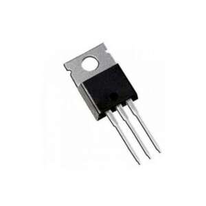
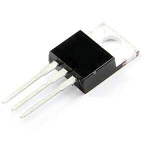
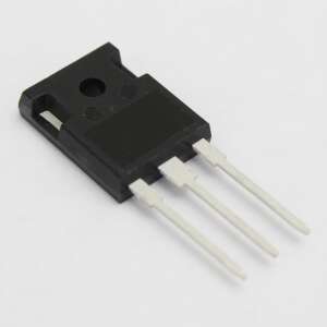
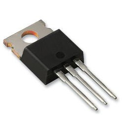
2SK2545 N-Channel MOSFET Transistor 600V 6A TO‑220
The 2SK2545 from Toshiba is an N‑channel enhancement‑mode MOSFET fabricated using π‑MOSV (planar) technology. It features a low drain‑source on‑resistance of 0.9 Ω (typical) and a high forward transfer admittance of 5.5 S (typical), enabling efficient power switching with low conduction losses. The device can handle drain‑source voltages up to 600 V and continuous drain current of 6 A (24 A pulsed). Its built‑in gate‑source protection and low leakage current (IDSS ≤ 100 µA at 600 V) make it suitable for high‑voltage switching regulators and offline power supplies.
The 2SK2545 is housed in a TO‑220 package (weight 1.9 g typ.) with a channel‑to‑case thermal resistance of 3.125 °C/W, allowing a maximum power dissipation of 40 W when properly heatsinked. It includes a fast body diode with reverse recovery time of 1000 ns (typical) for inductive load commutation. The device is rated for single‑pulse avalanche energy of 345 mJ, enhancing ruggedness in flyback or unclamped inductive switching applications. Typical applications include DC‑DC converters, relay and solenoid drivers, motor control, and general‑purpose high‑voltage switching where an N‑channel MOSFET with moderate current and high voltage capability is required.
Features:
- N‑channel enhancement mode (π‑MOSV technology).
- Very low drain‑source ON resistance.
- High forward transfer admittance.
- Low drain cut‑off current (high‑voltage leakage).
- Fast switching speeds (short turn‑on and turn‑off times).
- Built‑in gate‑source protection (Zener diode).
- Avalanche energy rated (single pulse).
- Suitable for high‑voltage DC‑DC conversion.
- Low total gate charge for efficient drive.
Specifications:
| Parameter | Symbol | Conditions | Min | Typ | Max | Unit |
|---|---|---|---|---|---|---|
| Drain-source voltage | VDSS | VGS = 0 V | 600 | – | – | V |
| Drain-gate voltage (RGS = 20 kΩ) | VDGR | – | 600 | – | – | V |
| Gate-source voltage | VGSS | – | ±30 | – | – | V |
| Drain current (DC) | ID | Tc = 25°C | – | – | 6 | A |
| Drain current (pulse) | IDP | Tc = 25°C | – | – | 24 | A |
| Drain power dissipation | PD | Tc = 25°C | – | – | 40 | W |
| Single pulse avalanche energy | EAS | VDD = 90V, L = 16.8mH, IAR = 6A | – | – | 345 | mJ |
| Avalanche current | IAR | – | – | – | 6 | A |
| Channel temperature | Tch | – | – | – | 150 | °C |
| Gate leakage current | IGSS | VGS = ±25V, VDS = 0V | – | – | ±10 | µA |
| Drain cut-off current | IDSS | VDS = 600V, VGS = 0V | – | – | 100 | µA |
| Drain-source breakdown voltage | V(BR)DSS | ID = 10mA, VGS = 0V | 600 | – | – | V |
| Gate threshold voltage | Vth | VDS = 10V, ID = 1mA | 2.0 | – | 4.0 | V |
| Drain-source ON resistance | RDS(ON) | VGS = 10V, ID = 3A | – | 0.9 | 1.25 | Ω |
| Forward transfer admittance | |Yfs| | VDS = 10V, ID = 3A | 2.0 | 5.5 | – | S |
| Input capacitance | Ciss | VDS = 10V, VGS = 0V, f = 1MHz | – | 1300 | – | pF |
| Reverse transfer capacitance | Crss | Same | – | 130 | – | pF |
| Output capacitance | Coss | Same | – | 400 | – | pF |
| Turn-on time | ton | VDD = 300V, ID = 3A, VGS = 10V, RL = 100Ω | – | 45 | – | ns |
| Turn-off time | toff | Same | – | 40 | – | ns |
| Total gate charge | Qg | VDD = 400V, VGS = 10V, ID = 6A | – | 150 | – | nC |
| Drain reverse current (continuous) | IDR | – | – | – | 6 | A |
| Diode forward voltage | VDSF | IDR = 6A, VGS = 0V | – | – | –1.7 | V |
| Reverse recovery time | trr | IDR = 6A, dIDR/dt = 100A/µs | – | 1000 | – | ns |

Pinout:

| Pin | Name | Description |
|---|---|---|
| 1 | Gate | Control terminal (MOSFET input) |
| 2 | Drain | Connected to metal tab (high voltage) |
| 3 | Source | Ground/return terminal |
Applications:
- DC‑DC converters (flyback, forward, boost).
- Relay and solenoid drivers.
- Motor drive circuits (brushed DC motors).
- Offline switching power supplies.
- High‑voltage switching regulators.
- Inductive load switching (with avalanche capability).
Packages:
- 1x 2SK2545 N-Channel MOSFET Transistor 600V 6A TO‑220.