Description
The CD405xB analog multiplexers and demuliplexers are digitally-controlled analog switches having low ON impedance and very low OFF leakage current. These multiplexer circuits dissipate extremely low quiescent power over the full VDD – VSS and VDD – VEE supply-voltage ranges, independent of the logic state of the control signals.
Features
- Wide Range of Digital and Analog Signal Levels
- Digital: 3 V to 20 V
- Analog: ≤20 VP-P
- Low ON Resistance,125 Ω (Typical) Over 15 VP-P Signal Input Range for VDD – VEE = 18 V
- High OFF Resistance, Channel Leakage of ±100 pA (Typical) at VDD– VEE = 18 V
- Logic-Level Conversion for Digital Addressing Signals of 3 V to 20 V (VDD – VSS = 3 V to 20 V) to Switch Analog Signals to 20 VP-P (VDD – VEE= 20 V) Matched Switch Characteristics, rON = 5 Ω (Typical) for VDD – VEE = 15 V Very Low Quiescent Power Dissipation Under All Digital-Control Input and Supply Conditions, 0.2 µW (Typical) at VDD – VSS = VDD – VEE = 10 V
- Binary Address Decoding on Chip
- 5 V, 10 V, and 15 V Parametric Ratings
- 100% Tested for Quiescent Current at 20 V
- Maximum Input Current of 1 µA at 18 V Over Full Package Temperature Range, 100 nA at 18 V and 25°C
- Break-Before-Make Switching Eliminates Channel Overlap
Specifications:
| Product Attribute | Attribute Value |
| Product Category: | Multiplexer Switch ICs |
| Series: | CD4053B |
| Mounting Style: | Through Hole |
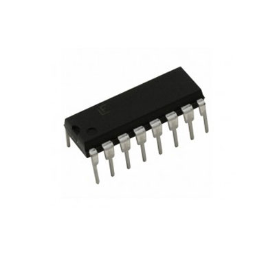
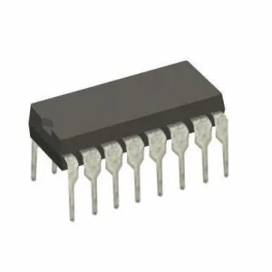
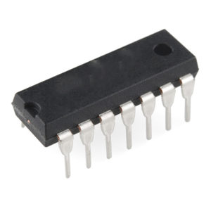
| Package/Case: | PDIP-16 |
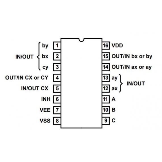
| Number of Channels: | 3 Channel |
| Configuration: | 3 x 2:1 |
| Supply Voltage – Min: | 5 V |
| Supply Voltage – Max: | 18 V |
| Minimum Dual Supply Voltage: | +/- 2.5 V |
| Maximum Dual Supply Voltage: | +/- 10 V |
| On Resistance – Max: | 240 Ohms |
| On Time – Max: | 720 ns |
| Off Time – Max: | 450 ns |
| Minimum Operating Temperature: | – 55 C |
| Maximum Operating Temperature: | + 125 C |
| Bandwidth: | 30 Mhz |
| Operating Supply Voltage: | 5 V to 18 V |
| Propagation Delay Time: | 60 ns |
| Supply Current – Max: | 100 uA |




Reviews
There are no reviews yet.