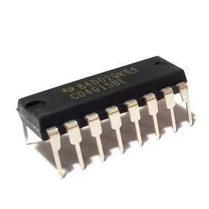

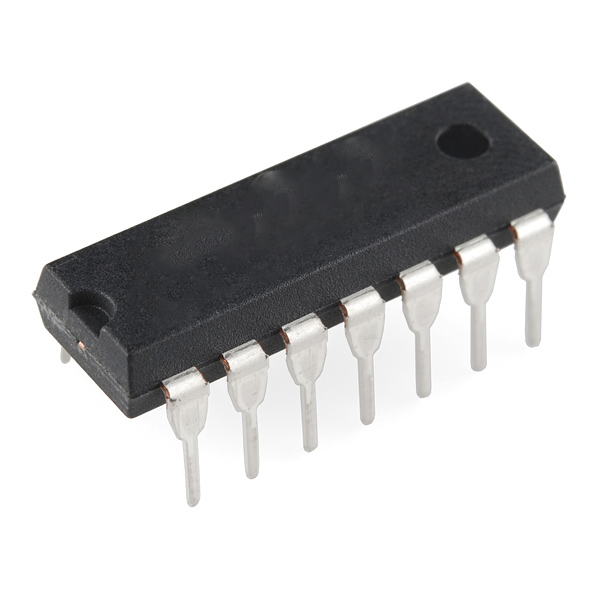

CD4069BE CMOS Hex Inverter/NOT Gate 3V to 18V 1µA PDIP-14
The CD4069UB device consists of six CMOS inverter circuits. These devices are intended for all general-purpose inverter applications where the medium-power TTL-drive and logic-level-conversion capabilities of circuits such as the CD4009 and CD4049 hex inverter and buffers are not required.
The CD4069UBE is supplied in a 14-pin PDIP package and operates from a recommended supply voltage range of 3 V to 18 V. It has standardized symmetrical output characteristics and medium-speed operation, with tPHL and tPLH of 30 ns typical at 10 V.
The device is designed for applications including logic inversion, pulse shaping, oscillators, and high-input-impedance amplifiers. Its lower drive capability also makes it suitable for driving light loads such as LEDs and helps reduce the chance of overshoots and undershoots.
Features
- Six CMOS inverter circuits in one package
- Standardized symmetrical output characteristics
- Wide recommended supply voltage range: 3 V to 18 V
- 100% tested for quiescent current at 20 V
- Maximum input current of 1 µA at 18 V over the full package-temperature range
- Recommended operating ambient temperature: -55°C to +125°C
Specifications
| Function | CMOS hex inverter |
|---|---|
| Number of inverter circuits | 6 |
| Package | PDIP-14, N package |
| Body size | 19.30 mm × 6.35 mm |
| Pin count | 14 |
| Recommended supply voltage, VDD | 3 V to 18 V |
| Absolute maximum supply voltage, VDD | -0.5 V to 20 V, stress rating only |
| Input voltage, all inputs, absolute maximum | -0.5 V to VDD + 0.5 V |
| Recommended operating ambient temperature | -55°C to +125°C |
| Storage temperature | -65°C to +150°C |
| Input current | 1 µA maximum at 18 V over full package-temperature range; 100 nA at 18 V and 25°C; static table limit ±1 µA maximum at VDD = 18 V |
| Quiescent device current at 25°C | 0.01 µA typical; 0.25 µA maximum at VDD = 5 V; 0.5 µA maximum at VDD = 10 V; 1 µA maximum at VDD = 15 V; 5 µA maximum at VDD = 20 V test condition |
| Propagation delay time, tPLH/tPHL | 30 ns typical at VDD = 10 V; 60 ns maximum at VDD = 10 V; 55 ns typical / 110 ns maximum at VDD = 5 V; 25 ns typical / 50 ns maximum at VDD = 15 V |
| Transition time, tTHL/tTLH | 50 ns typical / 100 ns maximum at VDD = 10 V; 100 ns typical / 200 ns maximum at VDD = 5 V; 40 ns typical / 80 ns maximum at VDD = 15 V |
| Input capacitance | 10 pF typical, 15 pF maximum |
| Low-level output voltage, VOL | 0.05 V maximum at VDD = 5 V, 10 V, or 15 V |
| High-level output voltage, VOH | 4.95 V minimum at VDD = 5 V; 9.95 V minimum at VDD = 10 V; 14.95 V minimum at VDD = 15 V |
| Input low voltage, VIL | 1 V maximum at VDD = 5 V; 2 V maximum at VDD = 10 V; 2.5 V maximum at VDD = 15 V |
| Input high voltage, VIH | 4 V minimum at VDD = 5 V; 8 V minimum at VDD = 10 V; 12.5 V minimum at VDD = 15 V |
| Output low sink current, IOL | VDD = 5 V: 0.51 mA minimum / 1 mA typical; VDD = 10 V: 1.3 mA minimum / 2.6 mA typical; VDD = 15 V: 3.4 mA minimum / 6.8 mA typical |
| Output high source current, IOH | VDD = 5 V: -0.51 mA minimum / -1 mA typical; VDD = 10 V: -1.3 mA minimum / -2.6 mA typical; VDD = 15 V: -3.4 mA minimum / -6.8 mA typical |
| Absolute maximum DC input current, any one input | -10 mA to +10 mA |
| Power dissipation | 500 mW per package from -55°C to 100°C; 100 mW per output transistor |
| Junction temperature | 150°C maximum |
| Lead temperature | 265°C maximum |

Applications
- Logic inversion
- Pulse shaping
- Oscillators
- High-input-impedance amplifiers
Package Content
- 1 x CD4069BE CMOS Hex Inverter/NOT Gate 3V to 18V 1µA PDIP-14