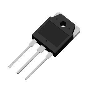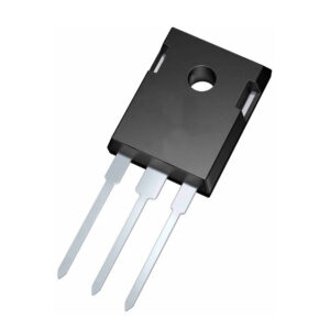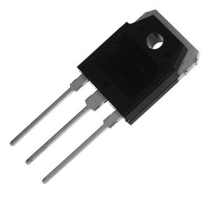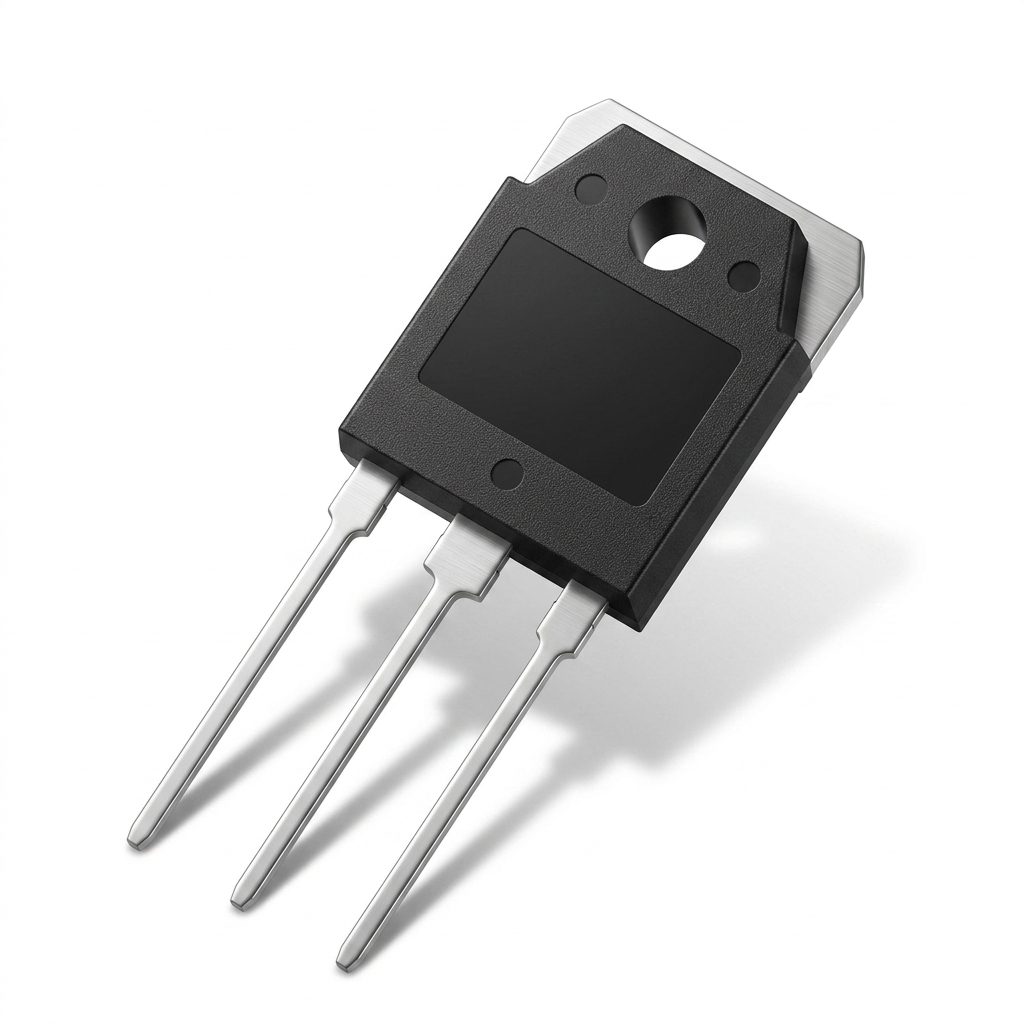
60T65PES High Speed IGBT 650V 100A TO-3P
60T65PES IGBT 650V 100A TO-3P. High-speed field stop trench IGBT with low loss for PFC, UPS, welder, and solar inverters.
120.00 EGP
Buy Now60T65PES High Speed IGBT 650V 100A TO-3P
The 60T65PES is a High Speed Fieldstop Trench IGBT from MagnaChip Semiconductor, produced using advanced MagnaChip Field Stop Trench IGBT 2nd Generation Technology. This device is designed to provide high efficiency switching behavior together with high ruggedness and excellent quality.
It is especially suitable for applications where low conduction losses are essential, including solar inverter, UPS, IH, welder, and PFC applications. The device supports a collector-emitter voltage of 650V and a DC collector current of 100A at TC = 25°C, with a pulsed collector current of 180A limited by maximum junction temperature.
The IGBT features low saturation voltage, low switching energy, high input impedance, and a maximum operating junction temperature of 175°C. Its diode section is specified with forward current ratings and reverse recovery characteristics, making it useful in high-speed power conversion circuits.
Features
- High Speed Switching and Low Power Loss
- VCE(sat) = 1.85V typical at IC = 60A
- Eoff = 0.53mJ at TC = 25°C
- High Input Impedance
- trr = 110ns typical at diF/dt = 500A/µs
- Maximum Junction Temperature 175°C
- Short circuit withstand time: 5µs under specified test conditions
- Low conduction loss for high-efficiency power applications
- Field Stop Trench IGBT, Second Generation technology
Specifications
| Parameter | Value | Conditions / Notes |
| Maximum Ratings | ||
| Collector-Emitter Voltage | 650 V | VCE |
| DC Collector Current | 100 A | TC = 25 °C, limited by Tvj max |
| DC Collector Current | 60 A | TC = 100 °C, limited by Tvj max |
| Pulsed Collector Current | 180 A | tp limited by Tvj max |
| Turn-Off Safe Operating Area | -180 A | VCE ≤ 650 V, Tvj ≤ 175 °C |
| Diode Forward Current | 60 A | TC = 25 °C, limited by Tvj max |
| Diode Forward Current | 30 A | TC = 100 °C, limited by Tvj max |
| Diode Pulsed Current | 200 A | tp limited by Tvj max |
| Gate-Emitter Voltage | ±20 V | VGE |
| Power Dissipation | 428 W | TC = 25 °C |
| Power Dissipation | 214 W | TC = 100 °C |
| Short Circuit Withstand Time | 5 µs | VCC ≤ 400 V, RG = 7 Ω, VGE = 15 V, Tvj = 150 °C |
| Operating Junction Temperature Range | -40 to 175 °C | Tvj |
| Storage Temperature Range | -55 to 150 °C | Tstg |
| Soldering Temperature | 260 °C | Wave soldering, 1.6 mm from case for 10 s |
| Mounting Torque | 0.6 Nm maximum | M3 screw |
| Thermal Characteristics | ||
| Thermal Resistance, Junction-to-Ambient | 40 °C/W | RθJA |
| Thermal Resistance, Junction-to-Case, IGBT | 0.35 °C/W | RθJC |
| Thermal Resistance, Junction-to-Case, Diode | 1.2 °C/W | RθJC |
| Static Electrical Characteristics | ||
| Collector-Emitter Breakdown Voltage | Min 650 V | IC = 2 mA, VGE = 0 V |
| Collector-Emitter Saturation Voltage | Typ 1.85 V, Max 2.4 V | IC = 60 A, VGE = 15 V, Tvj = 25 °C |
| Collector-Emitter Saturation Voltage | Typ 2.6 V | IC = 60 A, VGE = 15 V, Tvj = 175 °C |
| Diode Forward Voltage | Typ 1.45 V, Max 2.0 V | VGE = 0 V, IF = 25 A, Tvj = 25 °C |
| Diode Forward Voltage | Typ 1.35 V | VGE = 0 V, IF = 25 A, Tvj = 175 °C |
| Gate-Emitter Threshold Voltage | Min 4.0 V, Typ 5.0 V, Max 6.0 V | VCE = VGE, IC = 0.5 mA |
| Zero Gate Voltage Collector Current | Max 40 µA | VCE = 650 V, VGE = 0 V, Tvj = 25 °C |
| Gate-Emitter Leakage Current | Max ±100 nA | VGE = 20 V, VCE = 0 V |
| Dynamic Characteristics | ||
| Total Gate Charge | Typ 95 nC | VCE = 520 V, IC = 60 A, VGE = 15 V |
| Gate-Emitter Charge | Typ 19 nC | VCE = 520 V, IC = 60 A, VGE = 15 V |
| Gate-Collector Charge | Typ 47 nC | VCE = 520 V, IC = 60 A, VGE = 15 V |
| Input Capacitance | Typ 2327 pF | VCE = 25 V, VGE = 0 V, f = 1 MHz |
| Reverse Transfer Capacitance | Typ 55 pF | VCE = 25 V, VGE = 0 V, f = 1 MHz |
| Output Capacitance | Typ 270 pF | VCE = 25 V, VGE = 0 V, f = 1 MHz |
| Internal Emitter Inductance | Typ 13.0 nH | Measured 5 mm from case |
| Switching Characteristics at Tvj = 25 °C | ||
| Turn-On Delay Time | Typ 42 ns | VGE = 15 V, VCC = 400 V, IC = 60 A, RG = 7 Ω, Inductive Load |
| Rise Time | Typ 54 ns | VGE = 15 V, VCC = 400 V, IC = 60 A, RG = 7 Ω, Inductive Load |
| Turn-Off Delay Time | Typ 142 ns | VGE = 15 V, VCC = 400 V, IC = 60 A, RG = 7 Ω, Inductive Load |
| Fall Time | Typ 40 ns | VGE = 15 V, VCC = 400 V, IC = 60 A, RG = 7 Ω, Inductive Load |
| Turn-On Switching Energy | Typ 0.92 mJ | VGE = 15 V, VCC = 400 V, IC = 60 A, RG = 7 Ω, Inductive Load |
| Turn-Off Switching Energy | Typ 0.53 mJ | VGE = 15 V, VCC = 400 V, IC = 60 A, RG = 7 Ω, Inductive Load |
| Total Switching Energy | Typ 1.45 mJ | VGE = 15 V, VCC = 400 V, IC = 60 A, RG = 7 Ω, Inductive Load |
| Switching Characteristics at Tvj = 175 °C | ||
| Turn-On Delay Time | Typ 45 ns | VGE = 15 V, VCC = 400 V, IC = 60 A, RG = 7 Ω, Inductive Load |
| Rise Time | Typ 58 ns | VGE = 15 V, VCC = 400 V, IC = 60 A, RG = 7 Ω, Inductive Load |
| Turn-Off Delay Time | Typ 152 ns | VGE = 15 V, VCC = 400 V, IC = 60 A, RG = 7 Ω, Inductive Load |
| Fall Time | Typ 35 ns | VGE = 15 V, VCC = 400 V, IC = 60 A, RG = 7 Ω, Inductive Load |
| Turn-On Switching Energy | Typ 1.43 mJ | VGE = 15 V, VCC = 400 V, IC = 60 A, RG = 7 Ω, Inductive Load |
| Turn-Off Switching Energy | Typ 0.53 mJ | VGE = 15 V, VCC = 400 V, IC = 60 A, RG = 7 Ω, Inductive Load |
| Total Switching Energy | Typ 1.96 mJ | VGE = 15 V, VCC = 400 V, IC = 60 A, RG = 7 Ω, Inductive Load |
| Diode Reverse Recovery Characteristics at Tvj = 25 °C | ||
| Reverse Recovery Time | Typ 110 ns | IF = 25 A, diF/dt = 500 A/µs |
| Reverse Recovery Current | Typ 18 A | IF = 25 A, diF/dt = 500 A/µs |
| Reverse Recovery Charge | Typ 1.10 µC | IF = 25 A, diF/dt = 500 A/µs |
| Diode Reverse Recovery Characteristics at Tvj = 175 °C | ||
| Reverse Recovery Time | Typ 205 ns | IF = 25 A, diF/dt = 500 A/µs |
| Reverse Recovery Current | Typ 25 A | IF = 25 A, diF/dt = 500 A/µs |
| Reverse Recovery Charge | Typ 2.67 µC | IF = 25 A, diF/dt = 500 A/µs |
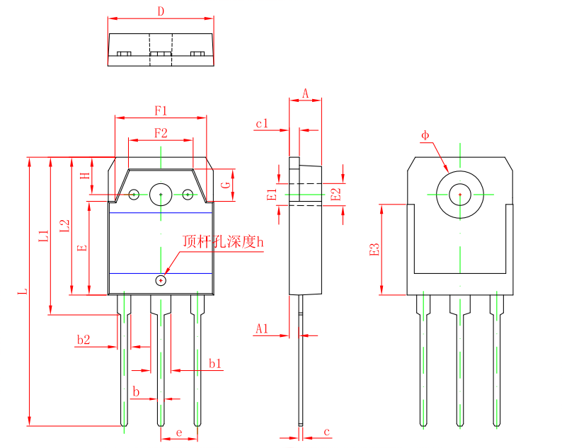

Applications
- Power Factor Correction (PFC) circuits.
- Uninterruptible Power Supplies (UPS).
- Photovoltaic (PV) inverters.
- Welding equipment.
- Induction Heating (IH) cookers.
DataSheet
Related products