74195 4-Bit Parallel-Access Shift Register
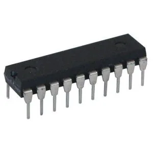
74195 4-bit parallel-access shift register enables efficient data shifting and storage with high-speed operation and easy integration in digital circuits.
25.00 EGP
Buy Now74195 4-Bit Parallel-Access Shift Register – Efficient Data Storage & Shifting Solution
Features:
- 4-bit parallel-access shift register
- Enables both parallel and serial data transfer
- High-speed operation for data shifting
- Versatile design for multiple logic applications
- Active low inputs for easy integration with other digital systems
- J, K Inputs to the First Stage
- Fully Synchronous Serial or Parallel Data Transfers
- Input Clamp Diodes Limit High-Speed Termination Effects
- Available in 16-pin PDIP, GDIP, and PDSO packages
Specifications:
Feature | Specification |
---|---|
Logic Family | CMOS |
Number of Bits | 4 |
Shift Register Type | Parallel-Access |
Clock Input | Active high (positive edge triggered) |
Input Type | Active Low |
Data Inputs | 4 parallel data inputs |
Shift Direction | Left or right (selectable) |
Output Type | Tri-state |
Operating Voltage Range | 3V to 15V |
Operating Temperature Range | 0°C to 70°C |
Package Type | Dual in-line package (DIP) |
Applications:
- Shift-left/right registers
- Sequence generation circuits
- Memory Defragmentation Circuits used in system repair

What is a Universal Shift Register?
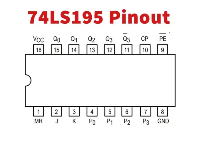
Universal Shift registers are an integral part of digital memory circuitry usually found in devices such as calculators, computers, and data processing systems. With a universal shift register, data or bits can be entered into the system in a serial or parallel manner. Data entry using 74LS195 is usually done from one direction, and as more data is added, it shifts positions until the data gets to the output end. The two ends are referred to as the left and right end. The movement of data can be from left to right, from right to left, or in both directions to make a bidirectional shift register.
74LS195 Pinout

74LS195 Pin Description
Pin No. | Pin Name | Description |
---|---|---|
1 | MR’ | Active Low Master Reset Input |
2 | J | First stage J Input |
3 | K’ | Active Low First Stage K Input |
4 | P0 | Parallel Data Input P0 |
5 | P1 | Parallel Data Input P1 |
6 | P2 | Parallel Data Input P2 |
7 | P3 | Parallel Data Input P3 |
8 | GND | Ground Pin |
9 | PE’ | Active Low Parallel Enable Input |
10 | CP | Clock Pulse Input |
11 | Q3′ | Complementary Last Stage Output |
12 | Q3 | Parallel Output Q3 |
13 | Q2 | Parallel Output Q2 |
14 | Q1 | Parallel Output Q1 |
15 | Q0 | Parallel Output Q0 |
16 | Vcc | Chip Supply Voltage |
Reviews
There are no reviews yet.