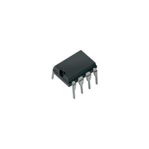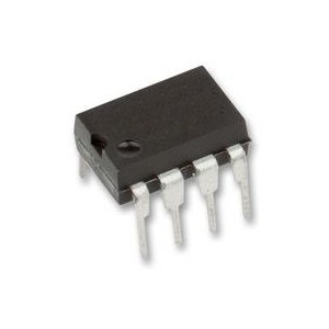
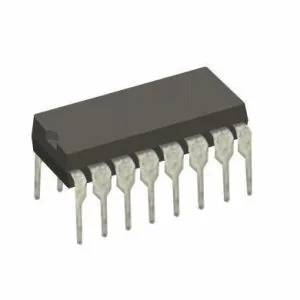





C3403C Quad Operational Amplifier 45nA PDIP-14
High-precision C3403C quad op-amp with ultra-low input bias (45 nA) in a 14-pin PDIP.
25.00 EGP
In stockSKU 3496300085378
Buy Now
Shipping across EgyptDelivered to your door
Cash on deliveryPay when your order arrives
Not sure it fits your project?Ask us on WhatsApp - we reply fast
C3403C Quad Operational Amplifier 45nA PDIP-14
The pPC3403 is a monolithic Quad Operational Amplifier consisting of four independent high-gain, internally frequency-compensated operational amplifiers, designed to operate from a single power supply or split power supplies over a wide range of voltages. The common mode input range includes the negative supply thereby eliminating the necessity for external biasing components in many applications.
Features
- Ultra-low input bias current: 45 nA typical
- Internal frequency compensation
- Common mode input voltage range includes V-
- Wide supply voltage range
- 3 V to 32 V (Single)
- 1.5 V to 16 V (Split)
- Class AB Output Stage for Minimal Crossover Distortion
- Output short circuit protection
Specification
Absolute Maximum Ratings
| Parameter | Symbol | μPC3403 | Unit |
|---|---|---|---|
| Voltage between V+ and V− (Note 1) | V+ − V− | −0.3 to +36 | V |
| Differential Input Voltage | VID | ±30 | |
| Input Voltage (Note 2) | VI | V− −0.3 to V+ +0.3 | |
| Output Voltage (Note 3) | VO | V− −0.3 to V+ +0.3 | |
| Power Dissipation (C Package) (Note 4) | PT | 570 | mW |
| Power Dissipation (G2 Package) (Note 5) | 550 | ||
| Operating Temperature Range | Topt | −20 to +80 | °C |
| Storage Temperature Range | Tstg | −55 to +125 |
- Note 1. Reverse connection of supply voltage can cause destruction.
- Note 2. The input voltage should be allowed to input without damage or destruction. Even during the transition period of supply voltage, power on/off, etc., this specification should be kept. Normal operation will establish when both inputs are within the Common Mode Input Voltage Range of electrical characteristics.
- Note 3. This specification is the voltage that may be applied to the output terminal from external sources without damage or destruction. Even during supply-voltage transitions, power on/off, etc., this specification should be kept. The output voltage of normal operation will be the Output Voltage Swing of the electrical characteristics.
- Note 4. Thermal derating factor is −7.6 mW/°C when ambient temperature is higher than 50 °C.
- Note 5. Thermal derating factor is −5.5 mW/°C when ambient temperature is higher than 25 °C.
- Note 6. Pay careful attention to the total power dissipation not to exceed the absolute maximum ratings, Note 4 and Note 5.
Recommended Operating Conditions
| Characteristic | Symbol | Min. | Typ. | Max. | Unit |
|---|---|---|---|---|---|
| Supply Voltage (Split) | V± | ±1.5 | – | ±16 | V |
| Supply Voltage (V– = GND) | V+ | +3 | – | +32 |
PINOUT

Dimensions

Applications
- Precision sensor interfaces (thermocouples, strain gauges).
- Battery-powered and portable instrumentation.
- Medical ECG/EEG front-end amplifiers.
- Low-current signal conditioning.
- Active filters and integrators.
- Data acquisition and precision measurement systems.
Documents
| Weight | 1 g |
|---|---|
| Dimensions | 19 × 9 × 8 mm |
Related products