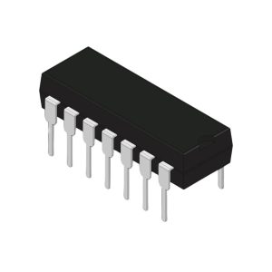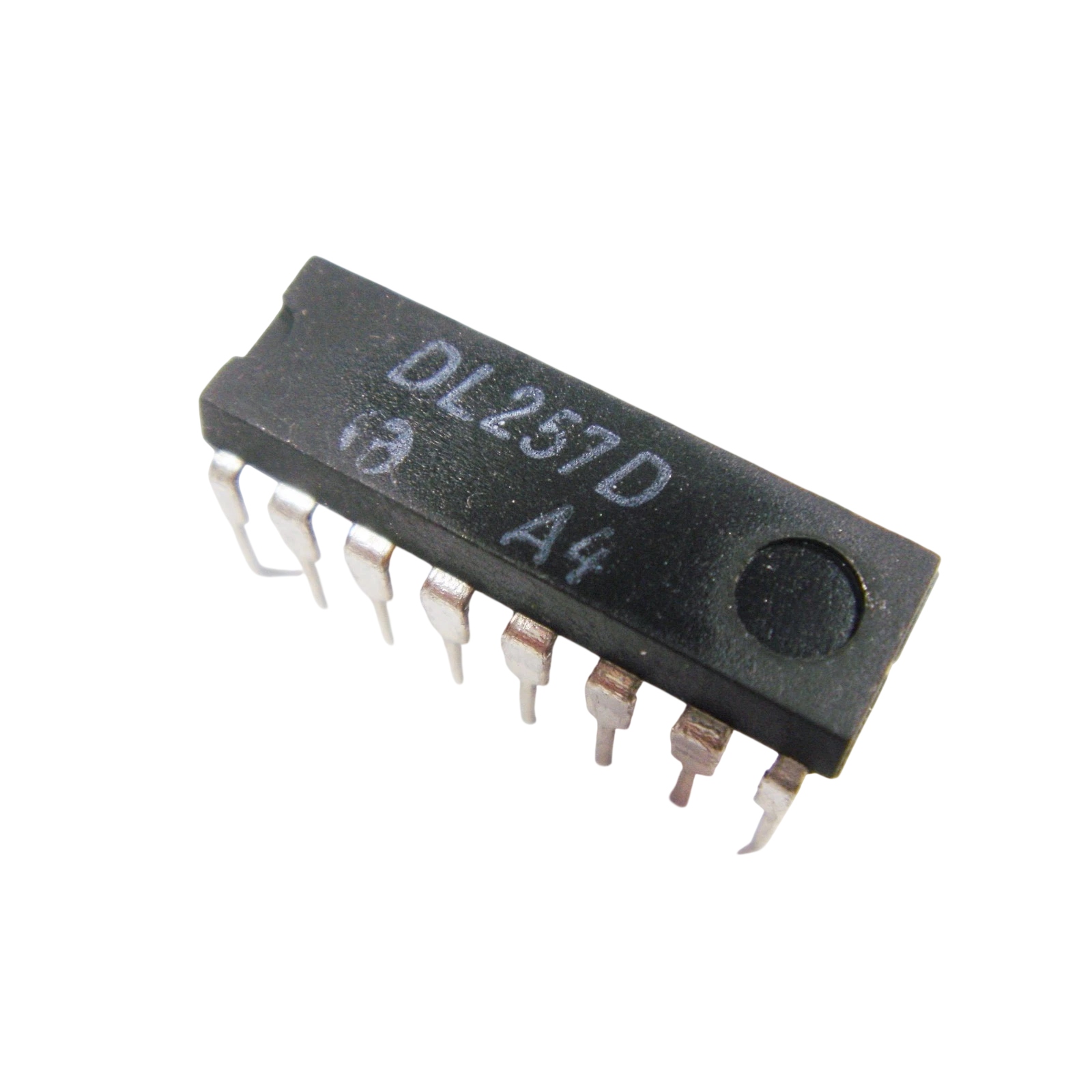
DL257D IC Quad 2-input multiplexer DIP-16
The DL257D is a TTL-based Quad 2-Input Data Selector/Multiplexer integrated circuit designed for digital signal routing, data selection, embedded systems, automation electronics, and logic control applications. The IC contains four independent 2-input multiplexers with common select and enable control lines inside a standard DIP16 through-hole package, making it suitable for breadboard prototyping, industrial electronics, educational projects, and PCB development.
Features:
- Four independent 2-input multiplexers.
- Compatible with 74257 and SN74LS257 IC families.
- Common select input control.
- 3-state output configuration.
- TTL Low-Power Schottky technology.
- Standard DIP16 through-hole package.
Specifications:
| Parameter | Value |
|---|---|
| Model | DL257D. |
| Equivalent IC | 74257 / 74LS257 / SN74LS257. |
| Technology | TTL Low-Power Schottky (LS). |
| Operating Voltage (VCC) | 5VDC (4.75V to 5.25V). |
| High‑Level Input Voltage (VIH) | Min 2.0V. |
| Low‑Level Input Voltage (VIL) | Max 0.8V. |
| High‑Level Output Voltage (VOH) | Min 2.7V (at IOH = -400µA). |
| Low‑Level Output Voltage (VOL) | Max 0.5V (at IOL = 8mA). |
| High‑Level Output Current (IOH) | -400µA. |
| Low‑Level Output Current (IOL) | 8mA. |
| Propagation Delay (A, B → Y) tPLH | 8ns typ, 21ns max. |
| Propagation Delay (A, B → Y) tPHL | 11ns typ, 21ns max. |
| Propagation Delay (S → Y) tPLH | 20ns typ, 32ns max. |
| Propagation Delay (S → Y) tPHL | 18ns typ, 25ns max. |
| Output Enable Time (OE → Y) tPZL | 13.5ns typ, 30ns max. |
| Output Enable Time (OE → Y) tPZH | 10.5ns typ, 25ns max. |
| Output Disable Time (OE → Y) tPLZ | 13ns typ, 30ns max. |
| Output Disable Time (OE → Y) tPHZ | 8.5ns typ, 26ns max. |
| Input Clamp Voltage (VIK) | 0.9V typ, 1.5V max. |
| Short‑Circuit Current (IOS) | 20mA min, 100mA max. |
| Operating Temperature | 0°C to +70°C. |
| Package Type | DIP-16. |

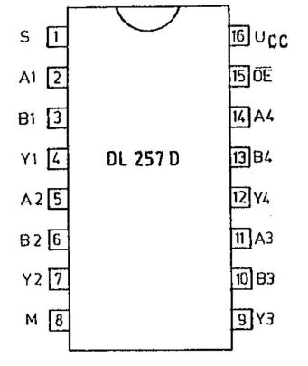
Pin Configuration:
| Pin Number | Pin Name | Function/Description |
|---|---|---|
| 1 | S (Select) | Common Select Input for all channels (LOW = select A, HIGH = select B). |
| 2 | A1 | Data Input A for Multiplexer 1. |
| 3 | B1 | Data Input B for Multiplexer 1. |
| 4 | Y1 | 3‑State Output for Multiplexer 1. |
| 5 | A2 | Data Input A for Multiplexer 2. |
| 6 | B2 | Data Input B for Multiplexer 2. |
| 7 | Y2 | 3‑State Output for Multiplexer 2. |
| 8 | GND | Ground (0V). |
| 9 | Y3 | 3‑State Output for Multiplexer 3. |
| 10 | B3 | Data Input B for Multiplexer 3. |
| 11 | A3 | Data Input A for Multiplexer 3. |
| 12 | Y4 | 3‑State Output for Multiplexer 4. |
| 13 | B4 | Data Input B for Multiplexer 4. |
| 14 | A4 | Data Input A for Multiplexer 4. |
| 15 | OE (Output Enable) | Common Output Enable Input (Active LOW). |
| 16 | VCC | Power Supply (+5V). |
Applications:
- Digital data routing systems.
- Bus-oriented electronic systems.
- Embedded logic control circuits.
- Microprocessor interfacing.
- Digital signal switching.
- Educational electronics projects.
- Breadboard prototyping.
- Industrial automation electronics.
- Data communication systems.
- Sequential logic circuits.
Package Include:
1x DL257D IC Quad 2-input multiplexer DIP-16