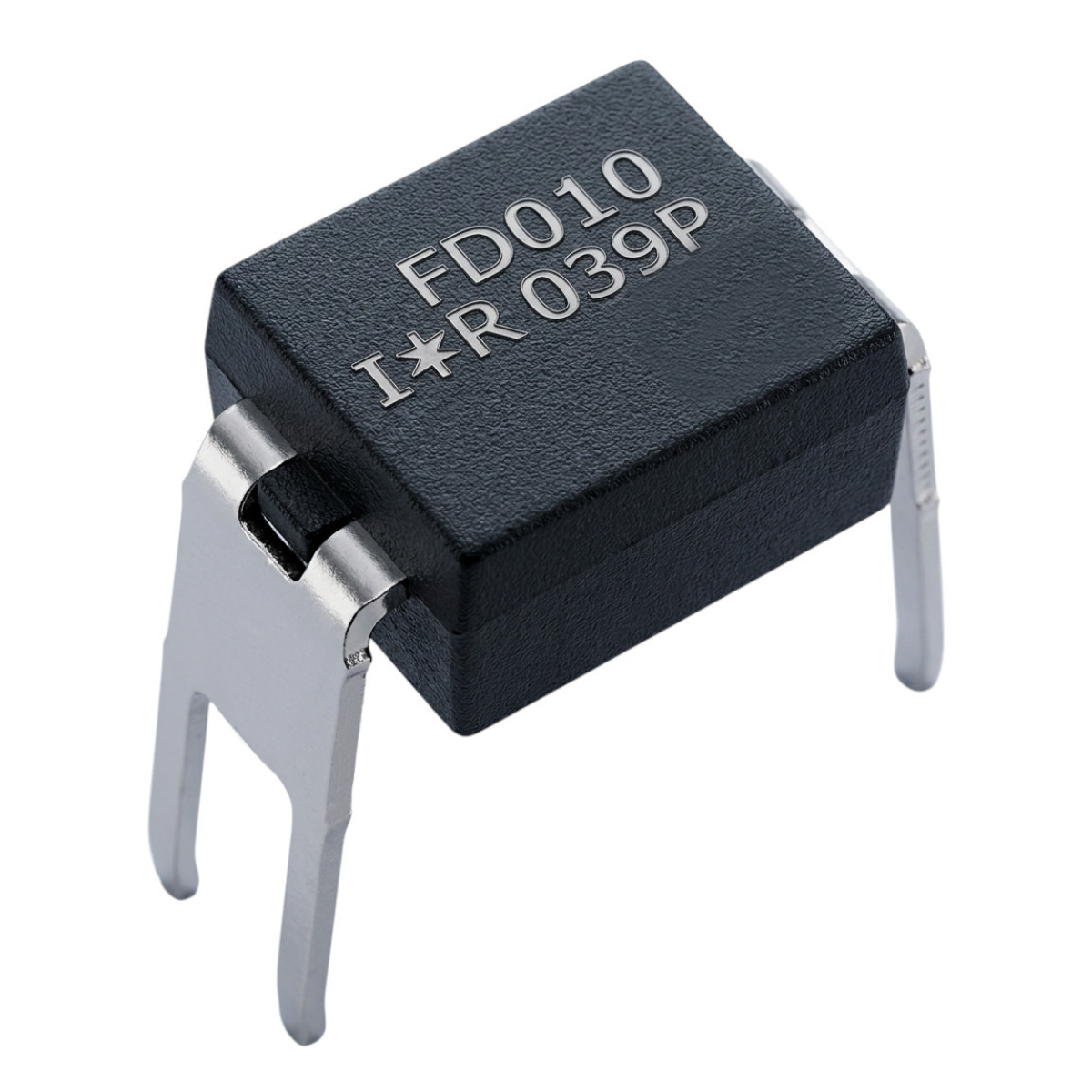
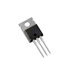
IRFD010 N-Channel HEXFET Power MOSFET 50V 1.7A DIP-4
The IRFD010 leverages advanced HEXFET technology to achieve very low on-state resistance combined with high transconductance and great device ruggedness. It inherits all the core advantages of standard MOSFETs, including simple voltage control, ultra-fast switching, ease of paralleling, and highly stable electrical parameters across temperature variations.
Features
- Optimized for Automatic Insertion
- Space-Saving Design
- High Efficiency
- Design Flexibility
- Robust Performance
Specifications
Absolute Maximum Ratings
| Symbol |
Parameter |
Value |
Units / Conditions |
| VDS |
Drain Source Voltage |
50 |
V |
| VDGR |
Drain Gate Voltage (RGS = 20 kΩ) |
50 |
V |
| ID @ 25°C |
Continuous Drain Current |
1.7 |
A, TC = 25°C |
| ID @ 100°C |
Continuous Drain Current |
1.1 |
A, TC = 100°C |
| IDM |
Pulsed Drain Current |
11 |
A |
| VGS |
Gate Source Voltage |
±20 |
V |
| PD @ 25°C |
Max. Power Dissipation |
1 |
W, TC = 25°C |
| – |
Linear Derating Factor |
0.0082 |
W/K (W/°C) |
| ILM |
Inductive Current, Clamped |
14 |
A, L = 100 μH |
| IL |
Unclamped Inductive Current (Avalanche Current) |
1.5 |
A |
| TJ, Tstg |
Operating Junction and Storage Temperature Range |
-55 to 150 |
°C |
| – |
Lead Temperature (Soldering) |
300 |
°C, 1.6mm from case for 10s |
Electrical Characteristics (@ TC = 25°C)
| Symbol |
Parameter |
Min |
Typ |
Max |
Units |
| BVDSS |
Drain Source Breakdown Voltage |
50 |
– |
– |
V (VGS = 0V, ID = 250 μA) |
| VGS(th) |
Gate Threshold Voltage |
2.0 |
– |
4.0 |
V (VDS = VGS, ID = 250 μA) |
| IGSS |
Gate-Source Leakage Forward |
– |
– |
500 |
nA (VGS = 20V) |
| IGSS |
Gate-Source Leakage Reverse |
– |
– |
-500 |
nA (VGS = -20V) |
| IDSS |
Zero Gate Voltage Drain Current |
– |
– |
250 |
μA (VDS = Max Rating, VGS = 0V) |
| IDSS |
High Temp. Zero Gate Voltage Drain Current |
– |
– |
1000 |
μA (0.8 × Max VDS, VGS = 0V, TC = 125°C) |
| ID(on) |
On-State Drain Current |
1.7 |
– |
– |
A (VDS > ID(on) × RDS(on)max, VGS = 10V) |
| RDS(on) |
Static Drain-Source On-State Resistance |
– |
0.16 |
0.20 |
Ω (VGS = 10V, ID = 0.88A) |
| gfs |
Forward Transconductance |
2.1 |
3.2 |
– |
S (VDS = 2 × VGS, IDS = 3.6A) |
Dynamic, Switching & Thermal Characteristics
| Symbol |
Parameter |
Min |
Typ |
Max |
Units |
| Ciss |
Input Capacitance |
– |
250 |
– |
pF (VGS = 0V, VDS = 25V, f = 1.0 MHz) |
| Coss |
Output Capacitance |
– |
150 |
– |
pF |
| Crss |
Reverse Transfer Capacitance |
– |
29 |
– |
pF |
| td(on) |
Turn-On Delay Time |
– |
11 |
17 |
ns (VDD = 25V, ID = 7.2A, RG = 25Ω, RD = 3.3Ω) |
| tr |
Rise Time |
– |
33 |
50 |
ns |
| td(off) |
Turn-Off Delay Time |
– |
12 |
18 |
ns |
| tf |
Fall Time |
– |
23 |
35 |
ns |
| Qg |
Total Gate Charge |
– |
8.8 |
13 |
nC (VGS = 10V, ID = 7.2A Max Rating) |
| Qgs |
Gate-Source Charge |
– |
2.2 |
3.3 |
nC |
| Qgd |
Gate-Drain (“Miller”) Charge |
– |
2.6 |
3.9 |
nC |
| LD |
Internal Drain Inductance |
– |
4.0 |
– |
nH (6mm from package to center of die) |
| LS |
Internal Source Inductance |
– |
6.0 |
– |
nH (6mm from package to source bonding pad) |
| RthJA |
Thermal Resistance, Junction-to-Ambient |
– |
120 |
– |
K/W (Typical socket mount) |
Source-Drain Diode Ratings & Characteristics
| Symbol |
Parameter |
Min |
Typ |
Max |
Units |
| IS |
Continuous Source Current (Body Diode) |
– |
– |
1.7 |
A |
| ISM |
Pulse Source Current (Body Diode) |
– |
– |
14 |
A |
| VSD |
Diode Forward Voltage |
– |
– |
1.6 |
V (TJ = 25°C, IS = 1.7A, VGS = 0V) |
| trr |
Reverse Recovery Time |
41 |
86 |
190 |
ns (TJ = 25°C, IF = 7.2A, dIF/dt = 100A/μs) |
| QRR |
Reverse Recovered Charge |
0.15 |
0.33 |
0.78 |
μC |
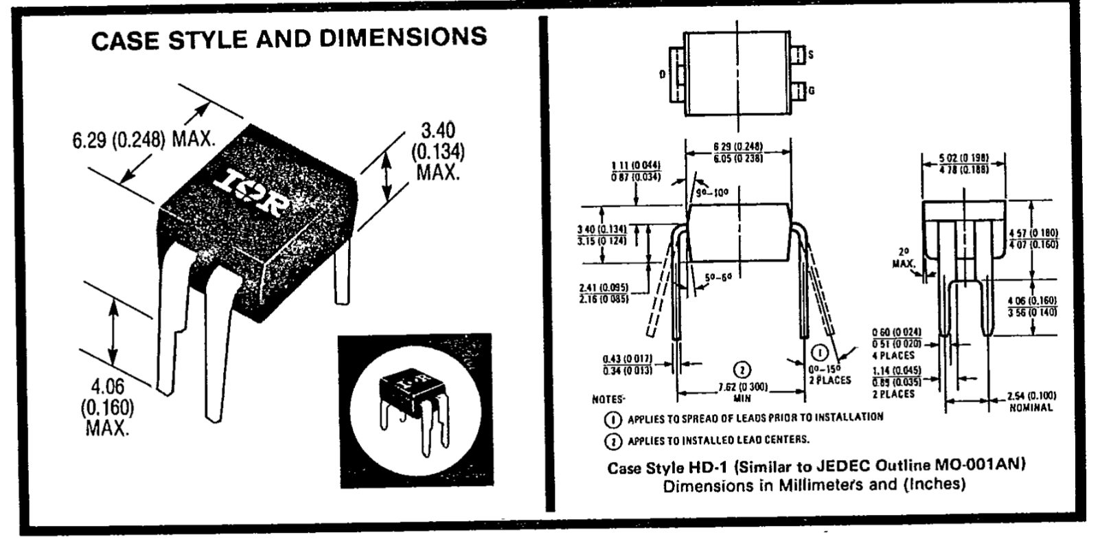
Applications
- Computer mainboards and peripheral circuit boards.
- Printers and office automation equipment.
- Telecommunications infrastructure and networking hardware.
- Consumer electronics and general-purpose power switching products.
Package Content
- 1 x IRFD010 N-Channel HEXFET Power MOSFET 50V 1.7A DIP-4
DataSheet