Features:
- Internally adjustable input offset voltage.
- Low power consumption.
- Wide common-mode (up to VCC+) and differential voltage range.
- Low input bias and offset current.
- Output short-circuit protection.
- High input impedance JFET input stage.
- Internal frequency compensation.
- Latch up free operation.
- High slew rate.
- Low input noise voltage.
- Low input noise current.
- Wide gain bandwidth.
- Low supply current.
- Low total harmonic distortion.
- High speed JFET input single operational amplifiers incorporating well matched, high voltage JFET and bipolar transistors in a monolithic integrated circuit.
Pin Configuration:

Specifications:
| Product Attribute | Attribute Value |
| Datasheet | LF351N |
| Product Category | Operational Amplifiers-Op Amps |
| Product | Operational Amplifiers |
| Number of Channels | 1 Channel |
| GBP – Gain Bandwidth Product | 4 MHz |
| SR – Slew Rate | 13 V/us |
| Vos – Input Offset Voltage(Max.) | 10 mV |
| Ib – Input Bias Current(Max.) | 200 pA |
| Supply Voltage – Max | 18 V |
| Supply Voltage – Min | – 18 V |
| Operating Supply Current | 3.4 mA |
| CMRR-Common Mode Rejection Ratio | 70 dB |
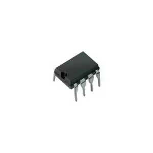
| Package/Case | DIP-8 |
| Mounting Style | Through Hole |
| Shutdown | No Shutdown |
| Minimum Operating Temperature | 0 °C to + 70 °C |
| Amplifier Type | Wideband Amplifier |
| Maximum Dual Supply Voltage | +/- 18 V |
| Pd – Power Dissipation | 500 mW (1/2 W) |
| PSRR – Power Supply Rejection Ratio | 70 dB |
| Supply Type | Dual |
| Voltage Gain dB | 100 dB |
Applications:
- Square Wave oscillator.
- High Q Notch Filter.
- Sample and Hold Circuit.
- In circuits that need high input impedance and high-speed integrators.
- Quick digital to analog converters.
- Sample and hold circuits, etc.


Reviews
There are no reviews yet.