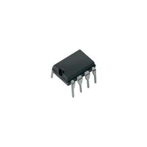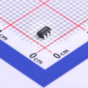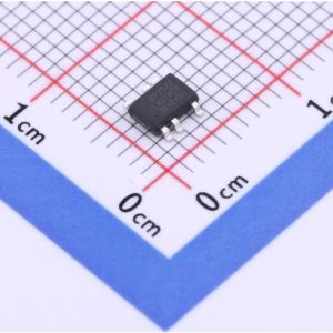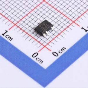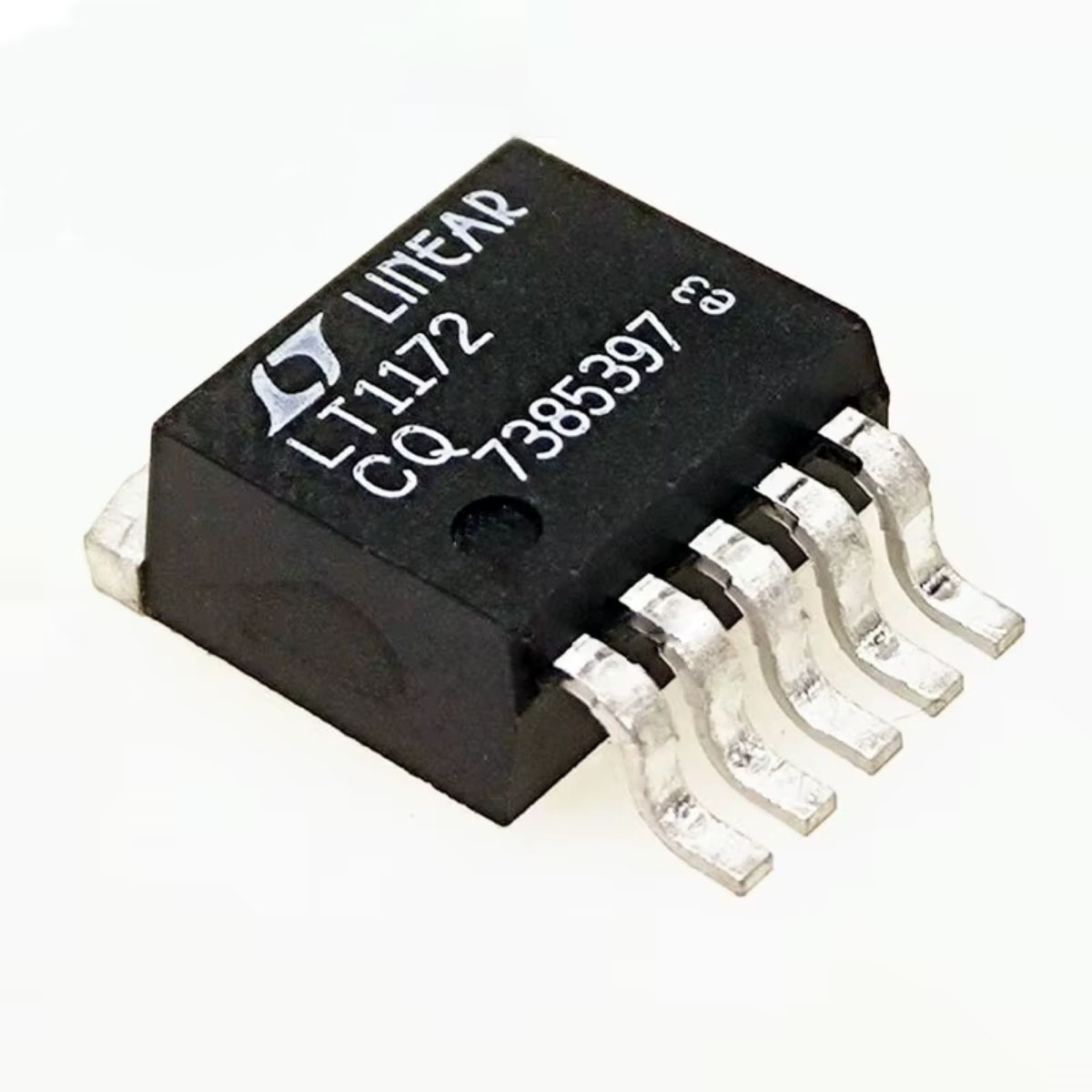
LT1172CQ SMD Switching Regulator 3V 1.25A 5-Lead DD Pak – Q
The LT1172CQ is a versatile monolithic switching regulator designed to provide efficient DC-DC power conversion in a wide range of electronic systems. It integrates a high-current power switch along with oscillator, control, and protection circuitry, making it suitable for boost (step-up), buck (step-down), and inverting converter configurations. Its flexible topology allows designers to build compact and reliable power supplies with minimal external components.
This IC is widely used in industrial control systems, automotive electronics, communication equipment, and embedded systems where stable and efficient voltage conversion is required. The LT1172CQ features internal current limiting and thermal protection, ensuring safe and reliable operation even under demanding conditions. Its surface-mount CQ package makes it ideal for modern PCB layouts requiring compact design and efficient thermal management.
Features:
- High-efficiency switching regulator.
- Supports boost, buck, and inverting topologies.
- Internal high-current power switch.
- Built-in oscillator.
- Internal current limiting protection.
- Thermal shutdown protection.
- Wide input voltage capability.
- Suitable for compact SMD designs.
Specifications:
| SYMBOL | PARAMETER | CONDITIONS | MIN | TYP | MAX | UNITS |
|---|---|---|---|---|---|---|
| VREF | Reference Voltage | Measured at Feedback Pin, VC=0.8V | 1.224 | 1.244 | 1.264 | V |
| IB | Feedback Input Current | VFB=VREF | 350 | 750 | nA | |
| gm | Error Amplifier Transconductance | ΔIC=±25μA | 2400 | 4400 | 7000 | mho |
| Error Amplifier Source or Sink Current | VC=1.5V | 120 | 200 | 400 | A | |
| Error Amplifier Clamp Voltage | Hi Clamp, VFB=1V | 1.80 | 2.30 | V | ||
| Lo Clamp, VFB=1.5V | 0.25 | 0.38 | 0.52 | V | ||
| Reference Voltage Line Regulation | 3V≤VIN≤VMAX
VC=0.8V |
0.03 | %/V | |||
| AV | Error Amplifier Voltage Gain | 0.9V ≤ VC ≤ 1.4V | 500 | 800 | V/V | |
| IQ | Supply Current | 3V ≤ VIN ≤ VMAX, VC = 0.6V | 6 | 9 | mA | |
| Control Pin Threshold | Duty Cycle = 0 | 0.6 | 0.9 | 1.25 | V | |
| Normal/Flyback Threshold on Feedback Pin | 0.4 | 0.45 | 0.54 | V | ||
| VFB | Flyback Reference Voltage (Note 5) | IFB=50μA | 14.0 | 16.3 | 18.0 | V |
| Change in Flyback Reference Voltage | 0.05≤IFB≤1mA | 4.5 | 6.8 | V | ||
| Flyback Reference Voltage Line Regulation (Note 5) | IFB=50μA
7V≤VIN≤VMAX |
0.01 | 0.03 | %/V | ||
| Flyback Amplifier Transconductance (gm) | ΔIC=±10μA | 150 | 300 | 650 | mho | |
| Flyback Amplifier Source and Sink Current | VC=0.6V (Source) | 15 | 32 | 70 | A | |
| IFB=50μA (Sink) | 25 | 40 | 70 | A | ||
| BV | Output Switch Breakdown Voltage | 3V≤VIN≤VMAX, ISW=1.5mA | 65 | 90 | V | |
| VSAT | Output Switch “On” Resistance (Note 3) | LT1170 | 0.15 | 0.24 | ||
| LT1171 | 0.30 | 0.50 | ||||
| LT1172 | 0.60 | 1.00 | ||||
| ILIM | Switch Current Limit (LT1170) | Duty Cycle = 50%, TJ≥25∘C | 5 | 10 | A | |
| Duty Cycle = 50%, TJ<25∘C | 5 | 11 | A | |||
| Duty Cycle = 80%, TJ<25∘C (Note 4) | 4 | 10 | A | |||
| Switch Current Limit (LT1171) | Duty Cycle = 50%, TJ≥25∘C | 2.5 | 5.0 | A | ||
| Duty Cycle = 50%, TJ<25∘C | 2.5 | 5.5 | A | |||
| Duty Cycle = 80%, TJ<25∘C (Note 4) | 2.0 | 5.0 | A | |||
| Switch Current Limit (LT1172) | Duty Cycle = 50%, TJ≥25∘C | 1.25 | 3.0 | A | ||
| Duty Cycle = 50%, TJ<25∘C | 1.25 | 3.5 | A | |||
| Duty Cycle = 80%, TJ<25∘C (Note 4) | 1.00 | 2.5 | A |

Pinout:
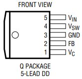
| Pin No. | Pin Name | Description |
|---|---|---|
| 1 | VC | Compensation Pin |
| 2 | Feedback | Feedback Input |
| 3 | GND | Ground |
| 4 | Switch | Internal Power Switch |
| 5 | VIN | Input Supply |
Applications:
- DC-DC Boost Converters.
- Buck Converters.
- Inverting Power Supplies.
- Industrial Power Systems.
- Automotive Electronics.
- Embedded Systems.
- Battery-Powered Devices.
- Communication Equipment.
Packages Included:
- 1x LT1172CQ SMD Switching Regulator 3V 1.25A 5-Lead DD Pak – Q.