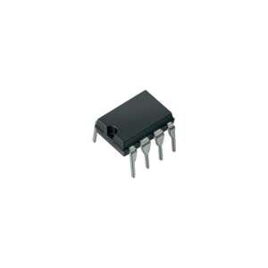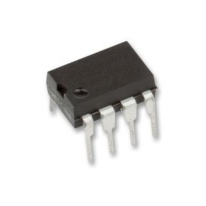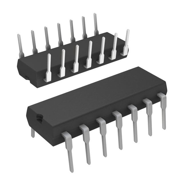
NE592N14 Video Amplifier 8V 10mA PDIP-14
NE592N14 Video Amplifier 8V 10mA PDIP-14 Features 120MHz bandwidth, fixed gains of 100/400, and 8V supply / 10mA output. Housed in a 14-pin package.
18.00 EGP
Buy NowNE592N14 Video Amplifier 8V 10mA PDIP-14
NE592N14 Video Amplifier 8V 10mA PDIP-14 is a monolithic, two-stage, differential output, wideband video amplifier housed in a 14-pin plastic Dual In-Line Package (DIP). It delivers high performance with selectable fixed gains of 100 and 400 without requiring external components, and its gain can be adjusted from 400 down to 0 using a single external resistor.
Features
- High-Speed Bandwidth
- Flexible Gain Control
- Integrated Filtering
- Simplified Design
- Efficient Wave Shaping
- High Reliability
Specifications
Absolute Maximum Ratings (TA = 25°C unless otherwise specified)
| Symbol | Parameter | Rating | Unit |
|---|---|---|---|
| VCC | Supply voltage | +8 | V |
| VIN | Differential input voltage | +5 | V |
| VCM | Common-mode input voltage | +6 | V |
| IOUT | Output current | 10 | mA |
| PDMAX | Maximum power dissipation, TA = 25°C (still air) [N-14 package] | 1.44 | W |
| TA | Operating ambient temperature range | 0 to +70 | °C |
| TSTG | Storage temperature range | -65 to +150 | °C |
DC Electrical Characteristics (VSS = ±6V, VCM = 0, Recommended VS = ±6.0V)
| Symbol | Parameter | Test Conditions | Min | Typ | Max | Unit |
|---|---|---|---|---|---|---|
| Differential Voltage Gain (Standard Part) | ||||||
| AVOL | Gain 1 (Pins G1A/G1B connected) | RL = 2kΩ, VOUT = 3VP-P, TA = 25°C | 250 | 400 | 600 | V/V |
| AVOL | Gain 1 (Pins G1A/G1B connected) | RL = 2kΩ, VOUT = 3VP-P, 0°C ≤ TA ≤ 70°C | 250 | – | 600 | V/V |
| AVOL | Gain 2 (Pins G2A/G2B connected) | RL = 2kΩ, VOUT = 3VP-P, TA = 25°C | 80 | 100 | 120 | V/V |
| AVOL | Gain 2 (Pins G2A/G2B connected) | RL = 2kΩ, VOUT = 3VP-P, 0°C ≤ TA ≤ 70°C | 80 | – | 120 | V/V |
| Input & Output Impedance / Range | ||||||
| RIN | Input resistance (Gain 1) | TA = 25°C | – | 4.0 | – | kΩ |
| RIN | Input resistance (Gain 2) | TA = 25°C | 10 | 30 | – | kΩ |
| RIN | Input resistance (Gain 2) | 0°C ≤ TA ≤ 70°C | 8.0 | – | – | kΩ |
| CIN | Input capacitance | Gain 2, TA = 25°C | – | 2.0 | – | pF |
| VIN | Input voltage range | 0°C ≤ TA ≤ 70°C | ±1.0 | – | – | V |
| ROUT | Output resistance | TA = 25°C | – | 20 | – | Ω |
| Offsets, Noise & Rejection Ratios | ||||||
| IOS | Input offset current | TA = 25°C / 0°C ≤ TA ≤ 70°C | – | 0.4 | 5.0 / 6.0 | μA |
| IBIAS | Input bias current | TA = 25°C / 0°C ≤ TA ≤ 70°C | – | 9.0 | 30 / 40 | μA |
| VNOISE | Input noise voltage | BW 1kHz to 10MHz, TA = 25°C | – | 12 | – | μVRMS |
| CMRR | Common-mode rejection ratio | Gain 2, VCM = ±1V, f < 100kHz, TA = 25°C | 60 | 86 | – | dB |
| CMRR | Common-mode rejection ratio | Gain 2, VCM = ±1V, f = 5MHz, TA = 25°C | 50 | 60 | – | dB |
| PSRR | Supply voltage rejection ratio | Gain 2, ΔVS = ±0.5V, TA = 25°C | – | 70 | – | dB |
| VOS | Output offset voltage (Gain 1) | RL = ∞, 0°C ≤ TA ≤ 70°C | – | – | 1.5 | V |
| VOS | Output offset voltage (Gain 2) | RL = ∞, 0°C ≤ TA ≤ 70°C | – | – | 1.5 | V |
| VOS | Output offset voltage (Gain 3 – all open) | RL = ∞, TA = 25°C / 0°C ≤ TA ≤ 70°C | – | 0.35 | 0.75 / 1.0 | V |
| Voltages & Supply Current | ||||||
| VCM | Output common-mode voltage | RL = ∞, TA = 25°C | 2.4 | 2.9 | 3.4 | V |
| VOUT | Output voltage swing differential | RL = 2kΩ, TA = 25°C / 0°C ≤ TA ≤ 70°C | 3.0 / 2.8 | 4.0 | – | V |
| ICC | Power supply current | RL = ∞, TA = 25°C / 0°C ≤ TA ≤ 70°C | – | 18 | 24 / 27 | mA |
AC Electrical Characteristics (TA = 25°C, VSS = ±6V, VCM = 0, VOUT = 1VP-P)
| Symbol | Parameter | Test Conditions | Min | Typ | Max | Unit |
|---|---|---|---|---|---|---|
| BW | Bandwidth | Gain 1 | 40 | – | – | MHz |
| BW | Bandwidth | Gain 2 | 90 | – | – | MHz |
| tr | Rise time | Gain 1 | – | 10.5 | – | ns |
| tr | Rise time | Gain 2 | – | 4.5 | – | ns |
| PD | Propagation delay | Gain 1 | – | 7.5 | 10 | ns |
| PD | Propagation delay | Gain 2 | – | 6.0 | 10 | ns |
Applications
- Floppy Disk Head Amplifier
- Video Amplifier
- Pulse Amplifier in Communications
- Magnetic Memory
- Video Recorder Systems
Package Content
- 1 x NE592N14 Video Amplifier 8V 10mA PDIP-14
DataSheet
Related products