- You cannot add "PIC12F675-I/P 8-Bit Microcontroller IC DIP-8" to the cart because the product is out of stock.
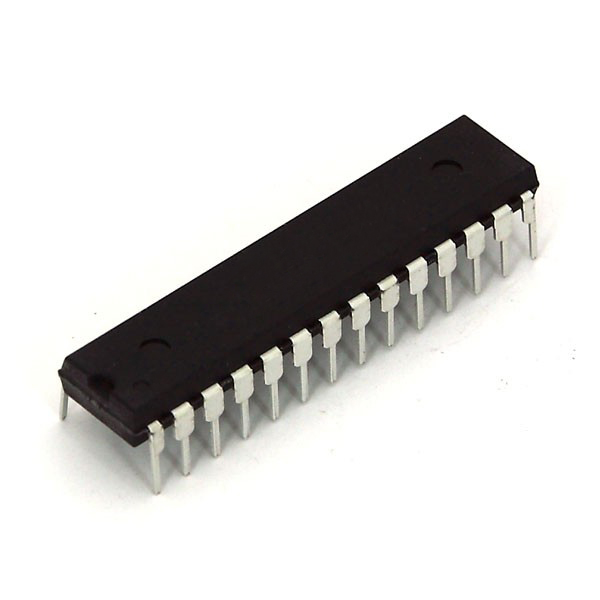
‘PIC’ is the popular microcontroller series from MICROCHIP and PIC18F2550 is one of the popular microcontroller from ‘PIC18F’ family. PIC18F2550 is a High-Performance, Enhanced flash, USB Microcontroller with NANO-Watt-Technology. This is an 8-bit microcontroller popular among makers and engineers due to its features and low cost. PIC18F2550 comes in various packages like DIP, QPF and QPN and can be selected according to the project requirement.
PIC18F2550 Pinout Configuration

It is a 28 pin IC as shown in PIC18F2550 pin diagram. There are so many features for a controller the manufacturer cannot provide I/O pins for each of them. So many pins of controller have multiple features. These features are disabled by default and can be enabled through programming. We will briefly describe functions of each pin below.
| Pin Number | Pin Name | Description |
| 1 | MCLR/VPP/RE3 | MCLR: Master Clear(RESET) Input
VPP:programming voltage input RE3: I/O pin of PORTE, PIN 3 |
| 2 | RA0/AN0 | RA0: I/O pin of PORTA, PIN 0
AN0: Analog input 0 |
| 3 | RA1/AN1 | RA1: I/O pin of PORTA, PIN 1
AN1: Analog input 1 |
| 4 | RA2/AN2/VREF-/CVREF | RA2: I/O pin of PORTA, PIN 2
AN2: Analog input 2 VREF-: A/D reference voltage (low) input CVREF: Analog comparator reference output |
| 5 | RA3/AN3/VREF+ | RA3: I/O pin of PORTA, PIN 3
AN3: Analog input3 VREF+: A/D reference voltage (high) input |
| 6 | RA4/T0CKI/C1OUT/RCV | RA4: I/O pin of PORTA, PIN 4
T0CKI: Timer0 external clock input C1OUT: Comparator 1 output RCV:External USB transceiver RCV input |
| 7 | RA5/AN4/SS/HLVDIN/C2OUT | RA5: I/O pin of PORTA, PIN 5
AN4: Analog input 4 SS: SPI slave select input HLDVIN: High/Low-Voltage Detect input C2OUT: Comparator 2 output |
| 8 | VSS | Ground |
| 9 | OSC1/CLKI | OSC1:Oscillator pin 1
CLKI: External clock source input |
| 10 | OSC2/CLKO/RA6 | OSC2: Oscillator pin 2
CLKO: clock source output RA6: I/O pin of PORTA, PIN 6 |
| 11 | RC0/T1OSO/T13CKI | RC0: I/O pin of PORTC, PIN 0
T1OSO :Timer1 oscillator output T13CKI: Timer1/Timer3 external clock input |
| 12 | RC1/T1OSI/CCP2/UOE | RC1: I/O pin of PORTC, PIN 1
T1OSI: Timer1 oscillator input CCP2:Capture 2 input/Compare 2 output/PWM2 output UOE: External USB transceiver OE output |
| 13 | RC2/CCP1 | RC2: I/O pin of PORTC, PIN 2
CCP1: Capture 1 input/Compare 1 output/PWM1 output. |
| 14 | VUSB | VUSB:Internal USB 3.3V voltage regulator output |
| 15 | RC4/D-/VM | RC4: I/O pin of PORTC, PIN 4
D-: USB differential minus line (input/output) VM: External USB transceiver VM input |
| 16 | RC5/D+/VP | RC5: I/O pin of PORTC, PIN 5
D+: USB differential plus line (input/output). VP: External USB transceiver VP input |
| 17 | RC6/TX/CK | RC6: I/O pin of PORTC, PIN 6
TX: EUSART asynchronous transmit CK: EUSART synchronous clock (see RX/DT). |
| 18 | RC7/RX/DT/SDO | RC7: I/O pin of PORTC, PIN 7
RX: EUSART asynchronous receive DT: EUSART synchronous data (see TX/CK). SDO: SPI data out |
| 19 | VSS | Ground |
| 20 | VDD | Positive Power Supply (+5V) |
| 21 | RB0/AN12/INT0/FLT0/SDI/SDA | RB0: I/O pin of PORTB, PIN 0
AN12: Analog input 12 INT0: External interrupt 0 FLT0: Enhanced PWM Fault input (ECCP1 module) SDI: SPI data in SDA: I2C data I/O |
| 22 | RB1/AN10/INT1/SCK/SCL | RB1: I/O pin of PORTB, PIN 1
AN10: Analog input 10 INT1: External interrupt 1 SCK: Synchronous serial clock input/output for SPI mode SCL: Synchronous serial clock input/output for I2C mode |
| 23 | RB2/AN8/INT2/VMO | RB2: I/O pin of PORTB, PIN 2
AN8: Analog input 8 INT2: External interrupt 2 VMO: External USB transceiver VMO output |
| 24 | RB3/AN9/CCP2/VPO | RB3: I/O pin of PORTB, PIN 3
AN9: Analog input 9 CCP2: Capture 2 input/Compare 2 output/PWM2 output VPO: External USB transceiver VPO output |
| 25 | RB4/AN11/KBI0 | RB4: I/O pin of PORTB, PIN 4
AN11: Analog input 11 KBI0: Interrupt-on-change pin |
| 26 | RB5/KBI1/PGM | RB5: I/O pin of PORTB, PIN 5
KBI1: Interrupt-on-change pin PGM: Low-Voltage ICSP Programming enable pin |
| 27 | RB6/KBI2/PGC | RB6: I/O pin of PORTB, PIN 6
KBI2: Interrupt-on-change pin PGC: In-Circuit Debugger and ICSP programming clock pin. |
| 28 | RB7/KBI3/PGD | RB7: I/O pin of PORTB, PIN 7
KBI3: Interrupt-on-change pin PGD: In-Circuit Debugger and ICSP programming data pin. |
PIC18F2550 Microcontroller Features
| PIC18F2550 – Simplified Features | |
| CPU | 8-bit |
| Total Number of Pins | 28 |
| Operating Voltage | +4.0 to +5.5 V (+5.5V being absolute maximum) |
| Number of programmable I/O pins | 24 |
| Communication Interface | USB Serial Interface (15,16 PINS) [Can be used for programming this controller]
Master/Slave SPI Serial Interface(7,18,21,22PINS) [Can be used for programming this controller] Programmable Serial UART(17,18PINS) [Can be used for programming this controller] Two-wire Serial Interface(21,22PINS)[Can be used to connect peripheral devices like sensors and LCDs] |
| ADC Module | 10channels, 10-bit resolution ADC |
| Timer Module | One8-bit counter, Three16-bit counter |
| Analog Comparators | 2 |
| PWM channels | 2 |
| External Oscillator | Up to 48MHz |
| Internal Oscillator | 32KHz-8MHz Calibrated Internal Oscillator |
| Program memory Type | Flash |
| Program memory / Flash memory | 32Kbytes[10000 write/erase cycles] |
| CPU Speed | 12 MIPS |
| RAM memory | 2KBytes |
| EEPROM memory | 256Bytes |
| Watchdog Timer | Programmable Watchdog Timer with Separate On-chipOscillator |
| Power Save Modes | Available |
| Operating Temperature | -40°C to +85°C(+85 being absolute maximum, -40 being absolute minimum) |
Note: Complete technical details can be found in the PIC18F2550 Datasheet linked at the bottom of this page.
Download:
- PIC18F2550 Data Sheet: PIC18F2550 Microcontroller Datasheet


Reviews
There are no reviews yet.