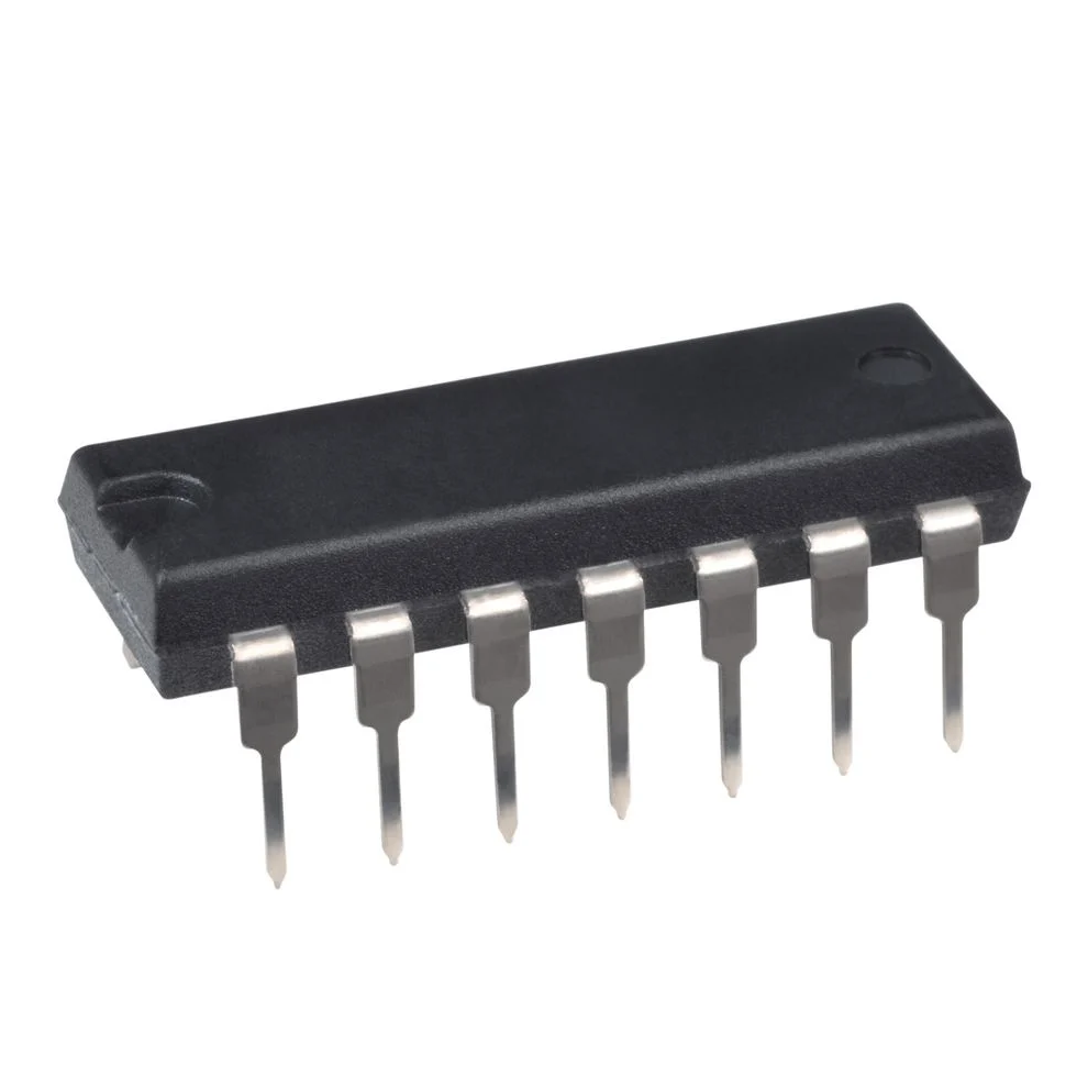
74LS242 Features
- Hysteresis at Inputs to Improve Noise Margin
- 2-Way Asynchronous Data Bus Communication
- PNP Inputs Reduce D-C Loading
74LS242 Pinout Diagram

74LS242 Pin Description
| Pin No | Pin Name | Description |
| 1 | GBA’ | Active Low Enable Pin |
| 2 | NC | Not Used |
| 3 | 1A | Channel 1 Of Transceiver (A) |
| 4 | 2A | Channel 2 Of Transceiver (A) |
| 5 | 3A | Channel 3 Of Transceiver (A) |
| 6 | 4A | Channel 4 Of Transceiver (A) |
| 7 | GND | Ground |
| 8 | 4B | Channel 4 Of Transceiver (B) |
| 9 | 3B | Channel 3 Of Transceiver (B) |
| 10 | 2B | Channel 2 Of Transceiver (B) |
| 11 | 1B | Channel 1 Of Transceiver (B) |
| 12 | NC | Not Used |
| 13 | GBA | Active High Enable pin |
| 14 | VCC | Positive Supply |
Product Attributes
| TYPE | DESCRIPTION |
| Category | Integrated Circuits (ICs) Logic Buffers, Drivers, Receivers, Transceivers |
| Series | 74LS |
| Logic Type | Transceiver, Inverting |
| Number of Elements | 1 |
| Number of Bits per Element | 4 |
| Current – Output High, Low | 15mA, 24mA |
| Voltage – Supply | 4.75V ~ 5.25V |
| Operating Temperature | 0°C ~ 70°C (TA) |
| Mounting Type | Through Hole |
| Package / Case | 14-DIP |
| Base Product Number | 74LS242 |


Reviews
There are no reviews yet.