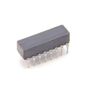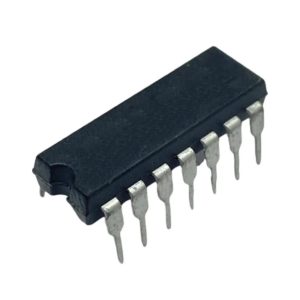



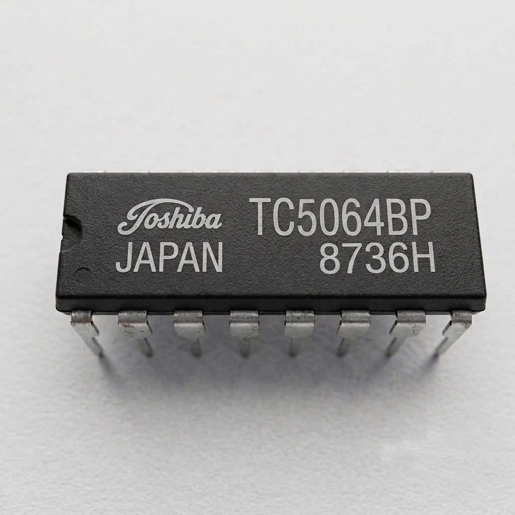
Toshiba TC5064BP Hex High-Voltage Buffer with Inhibit 3V to 18V 300mW DIP-16
Toshiba TC5064BP: Hex high-voltage buffer (non-inverting), 3V-18V supply, DIP-16 package. Ideal for driving fluorescent displays and PMOS logic interfacing.
75.00 EGP
In stockSKU 3496300155934
Buy Now
Shipping across EgyptDelivered to your door
Cash on deliveryPay when your order arrives
Not sure it fits your project?Ask us on WhatsApp - we reply fast
Toshiba TC5064BP Hex High-Voltage Buffer with Inhibit 3V to 18V 300mW DIP-16
The TC5064BP is a C2MOS digital integrated circuit containing six non-inverting buffer circuits with open-drain structure outputs. It features two common INHIBIT inputs (AIN, BIN) and is built using high-breakdown-voltage P-channel MOS FETs capable of withstanding up to -50V.
Designed for high-voltage output capabilities, the TC5064BP is an ideal solution for driving fluorescent display tubes and interfacing low-voltage logic with high-voltage MOS LSI circuits.
Features
- Type: Hex High Voltage Buffer (Non-Inverting Type)
- High Output Voltage Capability: Features P-channel MOS FETs with open-drain structure capable of -50V breakdown voltage
- Control Inputs: Includes two common INHIBIT inputs (AIN, BIN)
- Output Impedance Control: Supports High-Impedance (HZ) state via INHIBIT pin configurations
- Wide Operating Voltage Range: 3V to 18V
- Package: 16-pin Dual In-line Package (DIP-16 / 3D16A-P)
Specifications
1. Absolute Maximum Ratings (Ta = 25°C)
| Characteristic | Symbol | Rating | Unit |
|---|---|---|---|
| DC Supply Voltage | VDD | VSS – 0.5 ~ VSS + 20 | V |
| Input Voltage | VIN | VSS – 0.5 ~ VDD + 0.5 | V |
| Output Voltage | VOUT | VDD – 50 ~ VDD + 0.5 | V |
| Power Dissipation | PD | 300 | mW |
| DC Input Current | IIN | ±10 | mA |
| Storage Temperature Range | Tstg | -65 ~ 150 | °C |
| Lead Temp. / Time | Tsol | 260°C · 10sec | — |
2. Recommended Operating Conditions
| Characteristic | Symbol | Min. | Typ. | Max. | Unit |
|---|---|---|---|---|---|
| Supply Voltage | VDD | 3 | — | 18 | V |
| Input Voltage | VIN | 0 | — | VDD | V |
| Operating Temperature | Topr | -40 | — | 85 | °C |
3. Key Electrical Characteristics (VSS = 0V)
- High Level Output Current (IOH): Up to -35mA (at VDD = 15V, VOH = 12V at 25°C)
- Output OFF Current (IOFF): -10µA max at VOUT = VDD – 45V (25°C)
- Quiescent Supply Current (IDD): 0.005µA (Typ. at VDD = 5V, 25°C)
- Input Capacitance (CIN): 5pF (Typ.), 7.5pF (Max)
4. Truth Table (TC5064BP)
| Input (AIN) | Input (BIN) | Input (IN) | Output (TC5064BP) |
|---|---|---|---|
| L | H | L | HZ |
| L | H | H | H |
| * | L | * | HZ |
| H | * | * | HZ |
* HZ = High Impedance | * = Don’t care
Applications
- Fluorescent Display Tube Driving Circuits: Driving digit and segment signals for VFDs.
- Logic Level Translation: Interfacing between CMOS/TTL/NMOS and PMOS circuits.
- High-Voltage MOS LSI Interfacing: Buffer stage driving for circuits operating with high negative voltages (e.g., -EV).
Package Content
- 1 x Toshiba TC5064BP Hex High-Voltage Buffer with Inhibit 3V to 18V 300mW DIP-16
DataSheet
Related products