New
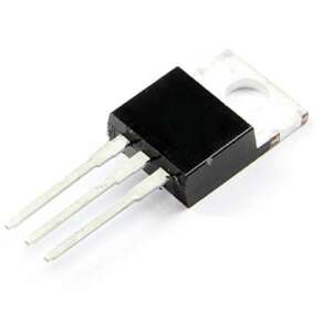
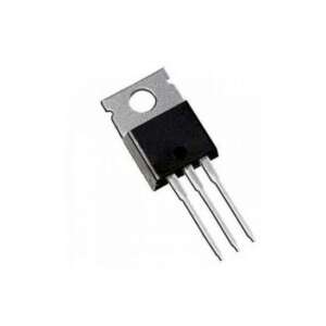
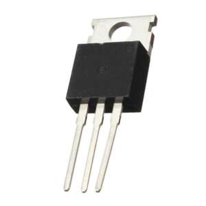
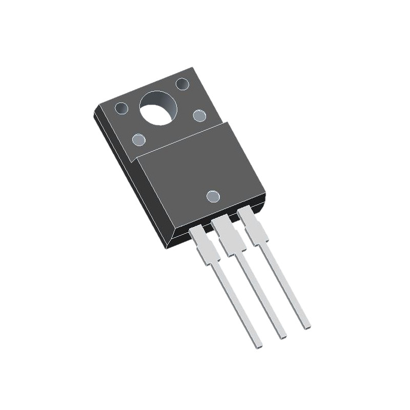
2SK2632 N-Channel MOSFET Transistor 800V 2.5A TO-220F
N-Channel MOSFET, 800V, 2.5A, TO-220F package. Ultrahigh-speed switching with low ON-resistance and low gate charge.
15.00 EGP
Buy Now2SK2632 N-Channel MOSFET Transistor 800V 2.5A TO-220F
The 2SK2632 is an N-channel silicon MOSFET designed for ultrahigh-speed switching applications. It blocks a minimum of 800V between drain and source and carries a continuous DC drain current of 2.5A (7.5A pulsed). Its two headline characteristics — low ON-resistance (RDS(on) = 3.6Ω typ. / 4.8Ω max. at VGS = 15V) and low total gate charge (Qg = 15nC typ.) — give it true nanosecond-class switching speed, with typical turn-ON delay and rise times of 15ns and turn-OFF delay and fall times of 45ns and 23ns respectively.
Features
- N-channel silicon MOSFET for ultrahigh-speed switching applications
- 800V minimum drain-to-source breakdown voltage
- 2.5A continuous (DC) drain current; 7.5A pulsed (PW ≤ 10µs, duty cycle ≤ 1%)
- Low ON-resistance: RDS(on) = 3.6Ω typ. / 4.8Ω max. (VGS = 15V, ID = 1.3A)
- Low total gate charge: Qg = 15nC typ. (VDS = 200V, VGS = 10V, ID = 2.5A)
- Very fast switching: td(on) = 15ns, tr = 15ns, td(off) = 45ns, tf = 23ns (typ.)
- Low capacitances: Ciss = 550pF, Coss = 150pF, Crss = 70pF (typ. at VDS = 20V, f = 1MHz)
- Very low leakage: IDSS ≤ 1.0µA (VDS = 800V); IGSS ≤ ±100nA (VGS = ±30V)
- Gate cutoff voltage 3.5V–5.5V; gate rating ±30V
- Built-in body diode: VSD = 0.84V typ. / 1.2V max. (IS = 2.5A)
- Power dissipation 2.0W (Ta = 25°C) / 25W (Tc = 25°C); channel temperature up to 150°C
- 3-pin TO-220FI-LS package; marking K2632
Specifications
Absolute Maximum Ratings (Ta = 25°C)
| Parameter | Symbol | Conditions | Rating | Unit |
|---|---|---|---|---|
| Drain-to-Source Voltage | VDSS | — | 800 | V |
| Gate-to-Source Voltage | VGSS | — | ±30 | V |
| Drain Current (DC) | ID | — | 2.5 | A |
| Drain Current (Pulse) | IDP | PW ≤ 10 µs, duty cycle ≤ 1% | 7.5 | A |
| Allowable Power Dissipation | PD | Ta = 25°C | 2.0 | W |
| Allowable Power Dissipation | PD | Tc = 25°C | 25 | W |
| Channel Temperature | Tch | — | 150 | °C |
| Storage Temperature | Tstg | — | –55 to +150 | °C |
Electrical Characteristics (Ta = 25°C)
| Parameter | Symbol | Test Conditions | Min | Typ | Max | Unit |
|---|---|---|---|---|---|---|
| Drain-to-Source Breakdown Voltage | V(BR)DSS | VGS = 0 V, ID = 1 mA | 800 | – | – | V |
| Zero Gate-Voltage Drain Current | IDSS | VGS = 0 V, VDS = 800 V | – | – | 1.0 | µA |
| Gate-to-Source Leakage Current | IGSS | VDS = 0 V, VGS = ±30 V | – | – | ±100 | nA |
| Cutoff Voltage | VGS(off) | VDS = 10 V, ID = 1 mA | 3.5 | – | 5.5 | V |
| Forward Transfer Admittance | |yfs| | VDS = 10 V, ID = 1.3 A | 0.7 | 1.4 | – | S |
| Static Drain-to-Source On-State Resistance | RDS(on) | VGS = 15 V, ID = 1.3 A | – | 3.6 | 4.8 | Ω |
| Input Capacitance | Ciss | VDS = 20 V, f = 1 MHz | – | 550 | – | pF |
| Output Capacitance | Coss | VDS = 20 V, f = 1 MHz | – | 150 | – | pF |
| Reverse Transfer Capacitance | Crss | VDS = 20 V, f = 1 MHz | – | 70 | – | pF |
| Total Gate Charge | Qg | VDS = 200 V, VGS = 10 V, ID = 2.5 A | – | 15 | – | nC |
| Turn-ON Delay Time | td(on) | Specified test circuit* | – | 15 | – | ns |
| Rise Time | tr | Specified test circuit* | – | 15 | – | ns |
| Turn-OFF Delay Time | td(off) | Specified test circuit* | – | 45 | – | ns |
| Fall Time | tf | Specified test circuit* | – | 23 | – | ns |
| Diode Forward Voltage | VSD | VGS = 0 V, IS = 2.5 A | – | 0.84 | 1.2 | V |

Applications
- Ultrahigh-speed / high-voltage switching circuits
- Fast switching power stages where low gate-charge drive and low ON-resistance losses are needed
- General high-voltage N-channel switch replacement
Package Content
- 1 x 2SK2632 N-Channel MOSFET Transistor 800V 2.5A TO-220F
DataSheet
Related products