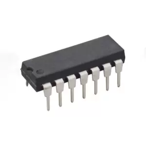
74266 Quad 2-Input Exclusive-NOR Gates
The 74×266 is a chip with four open-collector XNOR gates. This type of output makes it simple to connect it to other chips that use different logic levels. But it also means you can’t use this chip as a direct replacement for a normal XNOR gate chip.
In this guide, you will learn all about this chip and how you can use its XNOR gates in your own circuit.
What does the 74LS266 do?
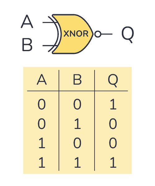
The 74×266 gives you four open-collector XNOR gates that can be used individually. An XNOR gate is a logic gate that outputs 1 (HIGH) if its inputs are equal (both 1 or both 0). In the truth table below, you can see what the output will be for any given input:
How To Use This Chip
The 74Ls266 comes in a 14-pin package, and you need to connect it to power before you can use it. Most 7400 ICs support a VCC voltage of 5V. One difference between the HC and LS versions of the chip is that the 74HC266 supports 2V to 6V, while the 74LS266 only supports 5V.
Once it’s connected, you can use any of the four open-collector XNOR gates inside.
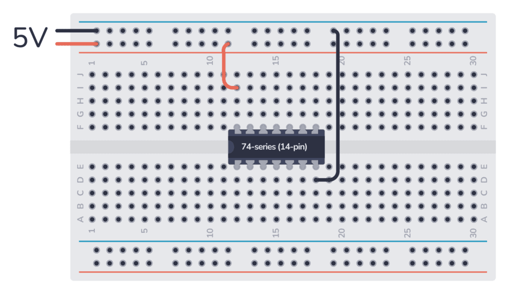
This chip uses open-collector outputs. That means you can only sink current (current can flow into the chip), not source it (current cannot flow out of the chip).
Each gate output of the 74HC266 can sink about 4 mA when powered with 5V. While the 74LS266 can usually sink about 8 mA of current. These values can vary between manufacturers of the chip though.
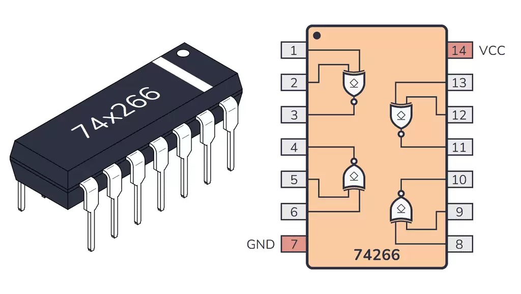
74×266 Pinout
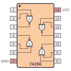
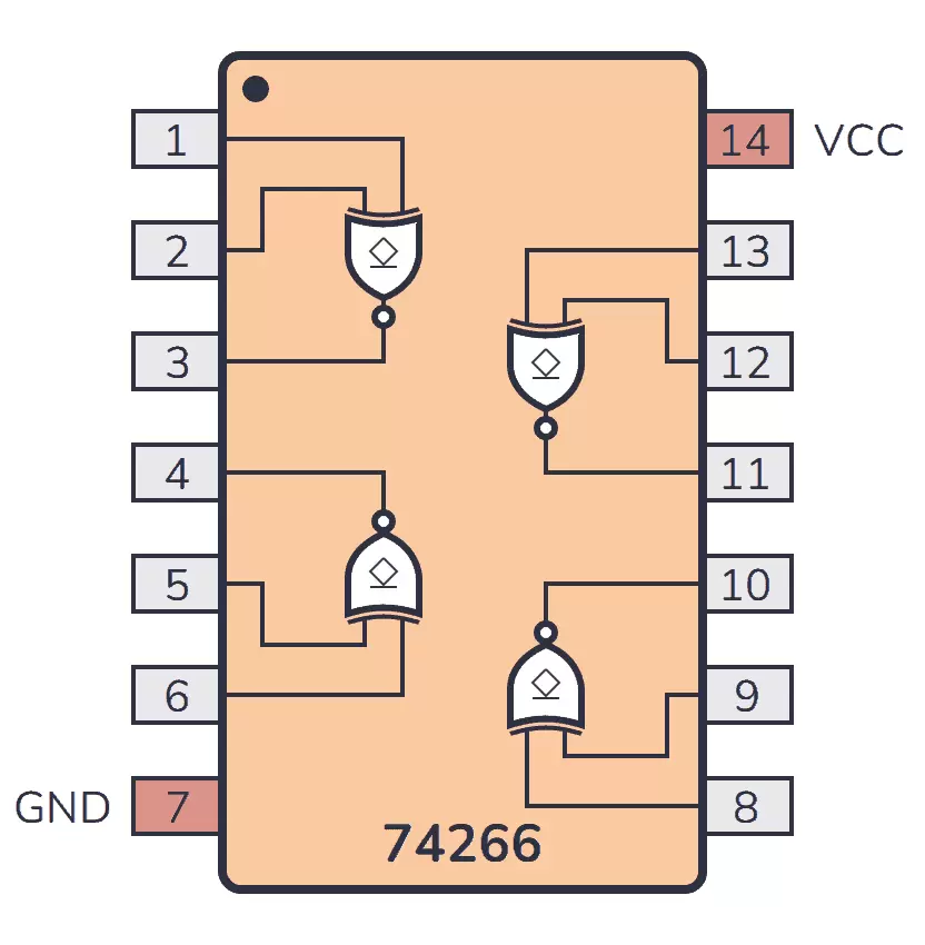
The 74×266 has 14 pins and contains four open-collector XNOR gates laid out as shown in the pinout diagram below. Each gate has the open-collector symbol, to remind you of the type of output:
| Pin # | Type | Description |
|---|---|---|
| 1 | Input | Input to the first XNOR gate. |
| 2 | Input | Input to the first XNOR gate. |
| 3 | Output | Open-collector output from the first XNOR gate. |
| 4 | Input | Input to the second XNOR gate. |
| 5 | Input | Input to the second XNOR gate. |
| 6 | Output | Open-collector output from the second XNOR gate. |
| 7 | Power | Connect to ground (GND). |
| 8 | Output | Open-collector output from the third XNOR gate. |
| 9 | Input | Input to the third XNOR gate. |
| 10 | Input | Input to the third XNOR gate. |
| 11 | Output | Open-collector output from the fourth XNOR gate. |
| 12 | Input | Input to the fourth XNOR gate. |
| 13 | Input | Input to the fourth XNOR gate. |
| 14 | Power | Positive power supply (VCC). Connect to +5V power. |
Technical Specifications
| Physical | |
| Case/Package | PDIP |
| Contact Plating | Gold |
| Mount | Through Hole |
| Number of Pins | 14 |
| Technical | |
| High-Level Output Current | -100 µA |
| Logic Function | XNOR |
| Low-Level Output Current | 8 mA |
| Max Operating Temperature | 70 °C |
| Max Output Current | 8 mA |
| Max Supply Voltage | 5.25 V |
| Min Operating Temperature | 0 °C |
| Min Supply Voltage | 4.75 V |
| Number of Bits | 4 |
| Number of Channels | 4 |
| Number of Circuits | 4 |
| Number of Elements | 4 |
| Number of Gates | 4 |
| Number of Input Lines | 2 |
| Number of Inputs | 2 |
| Number of Output Lines | 1 |
| Number of Outputs | 1 |
| Operating Supply Voltage | 5 V |
| Output Current | 8 mA |
| Propagation Delay | 30 ns |
| Quiescent Current | 8 mA |
| Termination | Through Hole |
| Turn-On Delay Time | 30 ns |


