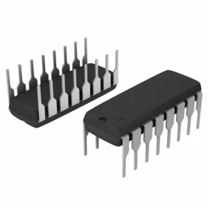
HYB41256-12 NMOS 256k x 1-Bit DRAM Memory IC Page Mode DIP-16
HYB41256-12 NMOS 256K x 1-Bit DRAM Memory IC Page Mode DIP-16 is a high-performance NMOS dynamic random-access memory organized as 262,144 × 1-bit. Designed for single 5V operation, it features page mode capability for faster sequential memory access by keeping the selected row active while changing only the column address. The device supports read, write, read-modify-write, hidden refresh, and RAS-only refresh operations, making it suitable for memory expansion, embedded systems, industrial equipment, and legacy computer hardware requiring reliable 256K-bit DRAM storage. Specifications are based on the uploaded datasheet.
Features
- 256K × 1-bit dynamic RAM organization.
- High-speed 120ns maximum access time.
- Supports Page Mode operation for faster sequential memory access.
- Single 5V power supply operation.
- Standard DIP-16 through-hole package.
- TTL-compatible input and output levels.
- Supports Read, Write, and Read-Modify-Write operations.
- Supports Hidden Refresh and RAS-only Refresh modes.
- Multiplexed address inputs reduce package pin count.
- Reliable NMOS memory technology.
- Suitable for legacy computer and industrial applications.
- Low standby power consumption.
Specifications
| Parameter | Details |
|---|---|
| Product Type | NMOS Page Mode DRAM Memory IC |
| Part Number | HYB41256-12 |
| Memory Organization | 256K × 1-Bit |
| Memory Capacity | 262,144Bits |
| Memory Type | Dynamic RAM (DRAM) |
| Technology | NMOS |
| Operating Mode | Page Mode |
| Access Time | 120ns |
| Supply Voltage | 5VDC |
| Operating Voltage Range | 4.5VDC to 5.5VDC |
| Package | DIP-16 |
| Address Inputs | 9 Multiplexed Address Lines |
| Input Compatibility | TTL Compatible |
| Refresh Modes | Hidden Refresh, RAS-only Refresh |
| Read / Write Modes | Read, Write, Read-Modify-Write |
| Operating Temperature | 0°C to +70°C |
Dimensions

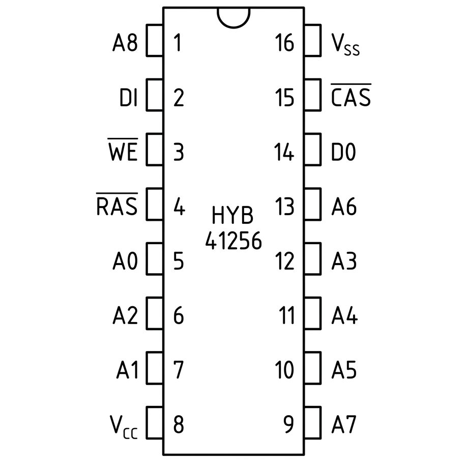
Pinout Configuration

| Pin Number | Pin Name | Function / Description |
|---|---|---|
| 1 | A8 | Address Input (Multiplexed). |
| 2 | DI | Data Input. |
| 3 | WE | Write Enable Input (Active Low). |
| 4 | RAS | Row Address Strobe Input (Active Low). |
| 5 | A0 | Address Input (Multiplexed). |
| 6 | A2 | Address Input (Multiplexed). |
| 7 | A1 | Address Input (Multiplexed). |
| 8 | VCC | Power Supply (+5V). |
| 9 | A7 | Address Input (Multiplexed). |
| 10 | A5 | Address Input (Multiplexed). |
| 11 | A4 | Address Input (Multiplexed). |
| 12 | A3 | Address Input (Multiplexed). |
| 13 | A6 | Address Input (Multiplexed). |
| 14 | DO | Data Output. |
| 15 | CAS | Column Address Strobe Input (Active Low). |
| 16 | VSS | Ground (0V). |
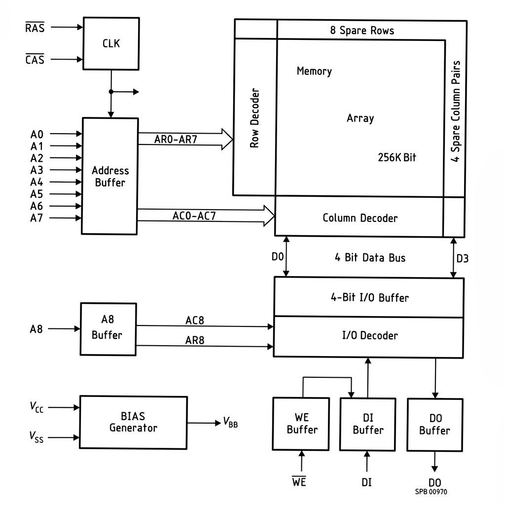
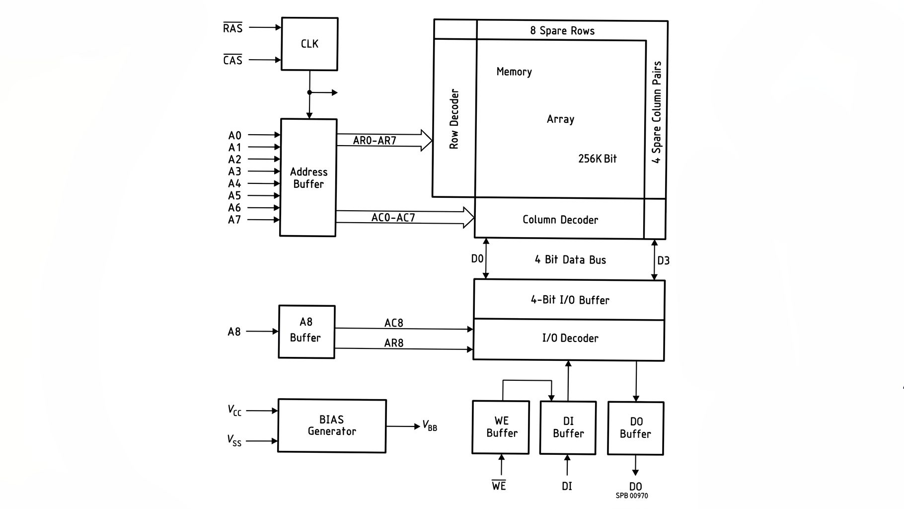
Connection Block Diagram
Applications
- Memory expansion for legacy computers.
- Embedded microprocessor systems.
- Industrial control equipment.
- Data acquisition systems.
- Telecommunications equipment.
- Test and measurement instruments.
- Digital controllers.
- Educational electronics projects.
- Computer repair and restoration.
- Electronic prototyping and development.
Package Contents
- 1 x HYB41256-12 NMOS 256k x 1-Bit DRAM Memory IC Page Mode DIP-16