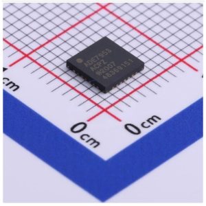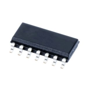


LMH6503MA Wideband Variable Gain Amplifier 1 Circuit ±5V ±75mA SOIC-14 SMD
The LMH6503MA from National Semiconductor is a wideband, DC-coupled, differential-input linear variable gain amplifier (VGA) consisting of a voltage-controlled gain stage followed by a high-speed current feedback op amp that can directly drive low-impedance loads.
The device provides a gain adjustment range of more than 70dB for frequencies up to 10MHz (79dB typical). Maximum gain is set by external components — anywhere from 1V/V to 100V/V or higher — and the gain can be reduced all the way to cut-off. Gain control is linear in V/V throughout the adjustment range, using a control voltage from −1V to +1V relative to pin 11 (ground pin). The gain control pin has high input impedance, simplifying its drive requirement.
Features
- −3dB bandwidth: 135MHz
- Gain control bandwidth: 100MHz
- Adjustment range (typical over temp): 70dB
- Gain matching (limit): ±0.7dB
- Slew rate: 1800V/µs
- Supply current (no load): 37mA
- Linear output current: ±75mA
- Output voltage (RL = 100Ω): ±3.2V
- Input voltage noise: 6.6nV/√Hz
- Input current noise: 2.4pA/√Hz
- THD (20MHz, RL = 100Ω, VO = 2VPP): −57dBc
Specifications
| PRODUCT INFORMATION | |
| Part Number | LMH6503MA |
| Product Type | Wideband, Low Power, Linear Variable Gain Amplifier (VGA) |
| Package | 14-Pin SOIC |
| Package Marking | LMH6503MA |
| Transport Media | 55 Units / Rail |
| OPERATING CONDITIONS | |
| Supply Voltage (V+ − V−) | 5V to 12V (±5V typical) |
| Operating Temperature Range | −40°C to +85°C |
| Storage Temperature Range | −65°C to +150°C |
| Power Consumption | 370mW |
| Thermal Resistance θJA (SOIC-14) | 138°C/W |
| Thermal Resistance θJC (SOIC-14) | 45°C/W |
| AC / DYNAMIC PERFORMANCE (VS = ±5V, TA = 25°C, RF = 1kΩ, RG = 174Ω, RL = 100Ω, AV(MAX) = 10; typical values) | |
| −3dB Bandwidth (VOUT < 0.5VPP) | 135 MHz |
| −3dB Bandwidth (AV(MAX) = 100) | 50 MHz |
| Gain Control Bandwidth | 100 MHz |
| Gain Flatness (±0.2dB, −1V < VG < +1V) | 40 MHz |
| Gain Adjustment Range (f < 10MHz) | 79 dB |
| Gain Adjustment Range (f < 30MHz) | 68 dB |
| Adjustment Range (typical over temp) | 70 dB |
| Attenuation Range (±0.2dB flatness, f < 30MHz) | 20 dB |
| Attenuation Range (±0.1dB flatness, f < 30MHz) | 6.6 dB |
| Gain Matching (limit, at maximum gain) | ±0.7 dB |
| Gain Accuracy (VG = +1V) | +0.25 dB (typ.) |
| Linear Phase Deviation (DC to 60MHz) | 1.6 deg |
| Group Delay (DC to 130MHz) | 2.6 ns |
| Feed-through (VG = −1.2V, 30MHz, output referred) | −48 dB |
| Rise and Fall Time (0.5V step) | 2.2 ns |
| Overshoot (0.5V step) | 10 % |
| Slew Rate (4V step) | 1800 V/µs |
| Gain Change Rate (10%–90% of final output) | 4.6 dB/ns |
| DISTORTION & NOISE PERFORMANCE | |
| 2nd Harmonic Distortion (HD2, 2VPP, 20MHz) | −60 dBc |
| 3rd Harmonic Distortion (HD3, 2VPP, 20MHz) | −61 dBc |
| Total Harmonic Distortion (THD, 2VPP, 20MHz) | −57 dBc |
| Total Equivalent Input Noise (1MHz to 150MHz) | 6.6 nV/√Hz |
| Input Noise Current (1MHz to 150MHz) | 2.4 pA/√Hz |
| Differential Gain (f = 4.43MHz, RL = 150Ω) | 0.15 % |
| Differential Phase (f = 4.43MHz, RL = 150Ω) | 0.22 deg |
| DC & INPUT/OUTPUT CHARACTERISTICS | |
| Supply Current (no load) | 37 mA (typ.), 50 mA (max.) |
| Supply Current (no load, VS = ±2.5V) | 12 mA (typ.) |
| Linear Output Current | ±75 mA (typ.) |
| Output Voltage Range (RL = 100Ω) | ±3.2 V (typ.) |
| Output Voltage Range (RL = open) | ±3.95 V (typ.) |
| Output Offset Voltage (−1V < VG < +1V) | ±80 mV (typ.), ±350 mV (max.) |
| Output Impedance (DC) | 0.1 Ω |
| Input Voltage Range (VCM, pins 3 & 6) | ±2.0 V (typ.) |
| Differential Input Voltage (pins 3 & 6) | ±0.34 V (typ.) |
| Input Resistance | 750 kΩ |
| Input Capacitance | 5 pF |
| Input Bias Current | 11 µA (typ.), 18 µA (max.) |
| Input Offset Current | 0.01 µA (typ.) |
| Gain Control (VG) Input Resistance | 70 kΩ |
| Gain Control (VG) Input Capacitance | 1.3 pF |
| Gain Control Voltage Range | −1V to +1V (relative to pin 11) |
| Maximum Gain Setting (via external components) | 1 V/V to 100 V/V or higher |
| Gain Multiplier (K) | 1.72 (typ.) |
| +Power Supply Rejection Ratio (+PSRR) | −80 dB (typ.) |
| −Power Supply Rejection Ratio (−PSRR) | −67 dB (typ.) |
| Common Mode Rejection Ratio (CMRR) | −67 dB (typ.) |
| ABSOLUTE MAXIMUM RATINGS | |
| Supply Voltage (V+ − V−) | 12.6 V |
| Input Current | ±10 mA |
| Output Current | 120 mA |
| Voltage at Input/Output Pins | V+ + 0.8V, V− − 0.8V |
| ESD Tolerance (Human Body Model) | 2 kV |
| ESD Tolerance (Machine Model) | 200 V |
| Junction Temperature | +150°C |
| Soldering Temperature (Infrared/Convection, 20 sec) | 235°C |
| Soldering Temperature (Wave, 10 sec) | 260°C |

Applications
- Variable attenuator
- AGC (Automatic Gain Control)
- Voltage-controlled filter
- Multiplier / four-quadrant multiplier
Package Content
- 1 x LMH6503MA Wideband Variable Gain Amplifier 1 Circuit ±5V ±75mA SOIC-14 SMD