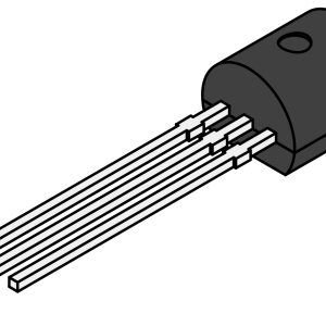
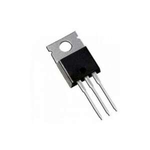
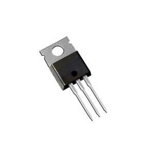
Toshiba K2362 N-Channel Power MOSFET 500V 10A TO-3PN
The K2362 is an N-channel power MOSFET designed for high-voltage switching applications. It features a 500 V drain-to-source voltage rating, ±10 A DC drain-current rating, ±30 V gate-to-source voltage rating, and low drain-to-source on-resistance of 1.0 Ω maximum at VGS = 10 V and ID = 5.0 A. The device also provides low input capacitance (Ciss = 1050 pF typical) and high avalanche capability ratings. The datasheet specifies a 100 W total power dissipation at Tc = 25 °C, with an MP-88 package and a 3-terminal electrical connection of Gate, Drain and Source; the package fin is connected to the Drain.
Features
- N-channel power MOSFET
- Designed for high-voltage switching applications
- Drain-to-source voltage: 500 V
- Low on-resistance: 1.0 Ω maximum at VGS = 10 V, ID = 5.0 A
- Low input capacitance: Ciss = 1050 pF typical
- High avalanche capability ratings
- Gate-to-source voltage rating: ±30 V
- DC drain current rating: ±10 A
- Pulsed drain current rating: ±40 A
- Total power dissipation: 100 W at Tc = 25 °C
- Single avalanche current: 10 A
- Single avalanche energy: 142 mJ
Specifications
| Specification | Value | Test Condition / Note |
|---|---|---|
| Part Number | K2362 | |
| Device Type | N-Channel Power MOS FET | Power MOS FET |
| Application Type | High-Voltage Switching | Industrial use |
| Package | MP-88 | Dimensions in millimeters |
| Drain-to-Source Voltage (VDSS) | 500 V | Absolute maximum rating for K2362 |
| Gate-to-Source Voltage (VGSS) | ±30 V | Absolute maximum rating |
| Drain Current, DC (ID) | ±10 A | Absolute maximum rating |
| Drain Current, Pulse | ±40 A | PW ≤ 10 µs, Duty Cycle ≤ 1% |
| Total Power Dissipation (PT1) | 100 W | Tc = 25 °C |
| Total Power Dissipation (PT2) | 3.0 W | Ta = 25 °C |
| Channel Temperature (Tch) | 150 °C | Maximum |
| Storage Temperature (Tstg) | -55 to +150 °C | Maximum rating |
| Drain-to-Source On-Resistance (RDS(on)) | 0.8 Ω min / 1.0 Ω max | VGS = 10 V, ID = 5.0 A |
| Gate-to-Source Cutoff Voltage (VGS(off)) | 2.5 to 3.5 V | VDS = 10 V, ID = 1 mA |
| Forward Transfer Admittance (|yfs|) | 3.0 S min | VDS = 10 V, ID = 5.0 A |
| Drain Leakage Current (IDSS) | 100 µA max | VDS = VDSS, VGS = 0 |
| Gate-to-Source Leakage Current (IGSS) | ±100 nA max | VGS = ±30 V, VDS = 0 |
| Input Capacitance (Ciss) | 1050 pF typ. | VDS = 10 V |
| Output Capacitance (Coss) | 200 pF typ. | VGS = 0, f = 1 MHz |
| Reverse Transfer Capacitance (Crss) | 26 pF typ. | VGS = 0, f = 1 MHz |
| Turn-On Delay Time (td(on)) | 15 ns typ. | VGS = 10 V, VDD = 150 V, RG = 10 Ω, RL = 30 Ω |
| Rise Time (tr) | 24 ns typ. | VGS = 10 V, VDD = 150 V, RG = 10 Ω, RL = 30 Ω |
| Turn-Off Delay Time (td(off)) | 50 ns typ. | VGS = 10 V, VDD = 150 V, RG = 10 Ω, RL = 30 Ω |
| Fall Time (tf) | 14 ns typ. | VGS = 10 V, VDD = 150 V, RG = 10 Ω, RL = 30 Ω |
| Total Gate Charge (QG) | 26 nC typ. | ID = 10 A, VDD = 400 V, VGS = 10 V |
| Gate-to-Source Charge (QGS) | 6.1 nC typ. | ID = 10 A, VDD = 400 V, VGS = 10 V |
| Gate-to-Drain Charge (QGD) | 12 nC typ. | ID = 10 A, VDD = 400 V, VGS = 10 V |
| Body Diode Forward Voltage (VF) | 1.0 V typ. | IF = 10 A, VGS = 0 |
| Reverse Recovery Time (trr) | 350 ns typ. | IF = 10 A, VGS = 0 |
| Reverse Recovery Charge (Qrr) | 2.0 µC typ. | di/dt = 50 A/µs, VGS = 0 |
| Single Avalanche Current (IAS) | 10 A | Starting Tch = 25 °C, RG = 25 Ω, VGS = 20 V → 0 V |
| Single Avalanche Energy (EAS) | 142 mJ | Starting Tch = 25 °C, RG = 25 Ω, VGS = 20 V → 0 V |

Applications
- High-voltage switching
- Industrial-use switching applications
Package Content
- 1 x Toshiba K2362 N-Channel Power MOSFET 500V 10A TO-3PN