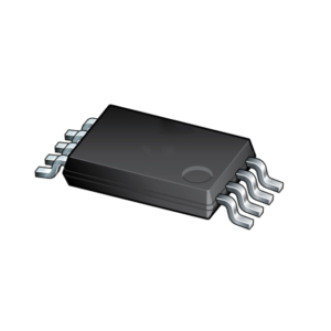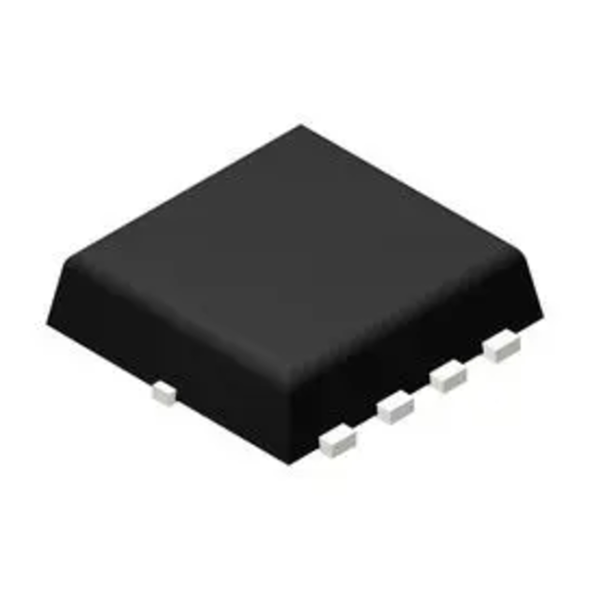

STL6P3LLH6 MOSFET Transistor P-CH -30V -25A PowerFLAT-8 (3.3×3.3) SMD
The STL6P3LLH6 is a P-Channel enhancement-mode power MOSFET designed using advanced trench technology to achieve low on-resistance, low gate charge, and efficient switching performance. Its compact PowerFLAT-8 (DFN3×3-8L) package makes it suitable for space-constrained electronic designs requiring high current handling and low power loss. The device operates with low gate drive voltages, making it compatible with modern battery-powered and portable electronic systems.
This MOSFET is widely used in battery protection circuits, load switching applications, DC power distribution systems, and uninterruptible power supplies. The combination of fast switching characteristics, low RDS(ON), and high current capability helps improve efficiency and reduce heat generation in power management designs. Its robust construction and wide operating temperature range make it suitable for consumer, industrial, and embedded electronic applications.
Features:
- P-Channel enhancement-mode MOSFET.
- Advanced trench technology.
- Low on-resistance design.
- Low gate charge for efficient switching.
- Fast switching performance.
- Suitable for low-voltage applications.
- Compact PowerFLAT-8 package.
- High current handling capability.
- Low power dissipation.
- Wide operating temperature range.
- Optimized for battery-powered systems.
- Suitable for power management circuits.
- Surface-mount package for automated assembly.
Specifications:
| Symbol | Parameter | Conditions | Min. | Typ. | Max. | Unit |
|---|---|---|---|---|---|---|
| BVDSS | Drain‑Source Breakdown Voltage | VGS=0V, ID=−250μA | -30 | — | — | V |
| BVDSS/ | BVDSS Temperature Coefficient | Reference to 25°C, ID=−1mA | — | -0.022 | — | V/°C |
| RDS(ON) | Static Drain‑Source On‑Resistance | VGS=−10V, ID=−15A | — | 16 | 20 | mΩ |
| VGS=−4.5V, ID=−10A | — | 22 | 32 | mΩ | ||
| VGS(th) | Gate Threshold Voltage | VGS=VDS, ID=−250μA | -1.0 | — | -2.5 | V |
| ΔVGS(th) | VGS(th) Temperature Coefficient | — | — | 4.6 | — | mV/°C |
| IDSS | Drain‑Source Leakage Current | VDS=−24V, VGS=0V, TJ=25 | — | — | -1 | µA |
| VDS=−24V, VGS=0V, TJ=55°C | — | — | -5 | µA | ||
| IGS | Gate‑Source Leakage Current | VGS=±25V, VDS=0V | — | — | ±100 | nA |
| Rg | Gate Resistance | VDS=0V, VGS=0V, f=1MHz | — | 13 | — | Ω |
| Qg | Total Gate Charge (-4.5V) | VDS=−15V, VGS=−4.5V, ID=−15A | — | 52 | — | nC |
| Qgd | Gate‑Drain Charge | — | — | 8.3 | — | nC |
| Td(on) | Turn‑On Delay Time | VDD=−15V, VGS=−10V, RG=3.3Ω, ID=−15A | — | 13 | — | ns |
| Tr | Rise Time | — | 15 | — | ns | |
| Td(off) | Turn‑Off Delay Time | — | — | 198 | — | ns |
| Tf | Fall Time | — | — | 98 | — | ns |
| Ciss | Input Capacitance | VDS=−15V, VGS=0V, f=1MHz | — | 1150 | — | pF |
| Coss | Output Capacitance | — | 150 | — | pF | |
| Crss | Reverse Transfer Capacitance | — | 134 | — | pF | |
| Is¹.⁵ | Continuous Source Current | VG=VDD=0V, Force Current | — | — | -32 | A |
| ISM².⁵ | Pulsed Source Current | — | — | — | -65 | A |
| VSD² | Diode Forward Voltage | VGS=0V, IS=−1A, TJ=25°C | — | — | -1.2 | V |
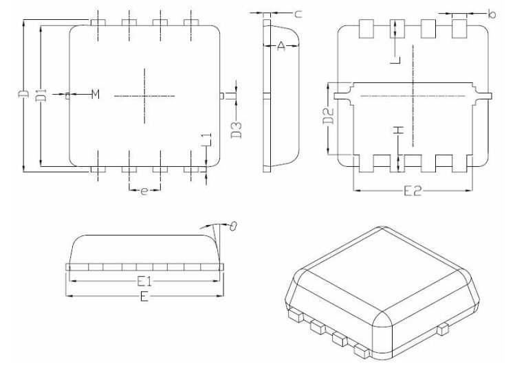
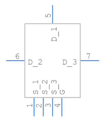
Pinout:
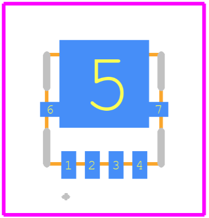
Footprint:
Applications:
- Battery protection circuits.
- Load switching circuits.
- Uninterruptible power supplies (UPS).
- Power path management.
- Portable electronics.
- DC power distribution.
- Battery-powered devices.
- Embedded systems.
- Power management modules.
- Automotive electronics.
- Industrial control equipment.
- High-side switching circuits.
Package Includes:
- 1x STL6P3LLH6 MOSFET Transistor P-CH -30V -25A PowerFLAT-8 (3.3×3.3) SMD.