-
-
-
-
-
-
-
-

-

-
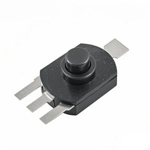
1612YD LED Flashlight ON-OFF Toggle Switch Push Button SPTT 12x15mm 4 Pin (4 PCS)
16.00 ج.م16.00 ج.م× -

-
-

-

-

-

ESP8266 Nodemcu with 0.96 OLED extended Temperature and Humidity Development Board
950.00 ج.م950.00 ج.م× -

-
-

-


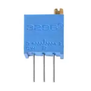





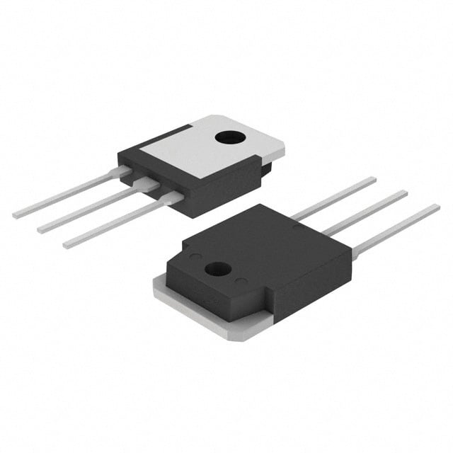
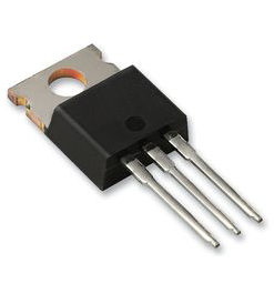
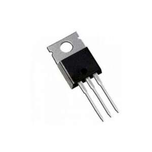
2SK2361 N-Channel Power MOSFET 450V 10A TO-3P
2SK2361 N-Channel Power MOSFET, 450V, 10A DC, RDS(on) 0.9Ω— designed for high-voltage industrial switching applications.
20.00 ج.م
متوفرالكود 3496300160693
اشترِ الآن
شحن لجميع محافظات مصريصلك حتى باب بيتك
الدفع عند الاستلامادفع عند وصول طلبك
غير متأكد أنه يناسب مشروعك؟اسألنا على واتساب - نرد بسرعة
2SK2361 N-Channel Power MOSFET 450V 10A TO-3P
The 2SK2361 is an N-Channel MOS Field Effect Transistor (Power MOS FET) manufactured by NEC Corporation, designed for high-voltage switching applications and rated for industrial use. The device blocks up to 450 V drain-to-source (VDSS) and handles a DC drain current of ±10 A (±40 A pulsed), with a total power dissipation of 100 W at a case temperature of 25 °C (3.0 W at 25 °C ambient).
It combines low on-resistance — RDS(on) of only 0.9 Ω maximum at VGS = 10 V, ID = 5.0 A — with low typical input capacitance (Ciss = 1050 pF) for fast, efficient switching, and high avalanche capability ratings (single avalanche current IAS = 10 A, single avalanche energy EAS = 142 mJ). A diode connected between gate and source serves as protection against ESD. The transistor is supplied in the MP-88 package, in which the metal fin (pin 4) is connected to the drain. The same datasheet also covers the companion device 2SK2362 (VDSS = 500 V, RDS(on) = 1.0 Ω max.).
Features
- N-Channel MOS field effect transistor for high-voltage switching (industrial use)
- Low on-resistance: RDS(on) = 0.9 Ω max. (VGS = 10 V, ID = 5.0 A)
- Low input capacitance: Ciss = 1050 pF typ.
- High avalanche capability ratings (IAS = 10 A, EAS = 142 mJ)
- High voltage blocking: VDSS = 450 V; VGSS = ±30 V
- High current capability: ID = ±10 A (DC), ±40 A (pulse)
- Power dissipation: 100 W (TC = 25 °C) / 3.0 W (TA = 25 °C)
- Fast switching: td(on) = 15 ns, tr = 24 ns, td(off) = 50 ns, tf = 14 ns (typ.)
- Low total gate charge: QG = 26 nC (typ.)
- Built-in gate–source diode for ESD protection
Specifications
Absolute Maximum Ratings (TA = 25°C)
| Parameter | Symbol | Rating | Unit | Conditions / Notes |
|---|---|---|---|---|
| Drain to Source Voltage | VDSS | 450 | V | 2SK2361 (companion 2SK2362: 500 V) |
| Gate to Source Voltage | VGSS | ±30 | V | |
| Drain Current (DC) | ID (DC) | ±10 | A | |
| Drain Current (Pulse) | ID (pulse) | ±40 | A | PW ≤ 10 µs, Duty Cycle ≤ 1 % |
| Total Power Dissipation | PT1 | 100 | W | TC = 25 °C |
| Total Power Dissipation | PT2 | 3.0 | W | TA = 25 °C |
| Channel Temperature | Tch | 150 | °C | |
| Storage Temperature | Tstg | -55 to +150 | °C | |
| Single Avalanche Current | IAS | 10 | A | Starting Tch = 25 °C, RG = 25 Ω, VGS = 20 V → 0 |
| Single Avalanche Energy | EAS | 142 | mJ | Starting Tch = 25 °C, RG = 25 Ω, VGS = 20 V → 0 |
Electrical Characteristics (TA = 25°C)
| Characteristic | Symbol | Min. | Typ. | Max. | Unit | Test Conditions |
|---|---|---|---|---|---|---|
| Drain to Source On-Resistance | RDS(on) | – | 0.7 | 0.9 | Ω | VGS = 10 V, ID = 5.0 A |
| Gate to Source Cutoff Voltage | VGS(off) | 2.5 | – | 3.5 | V | VDS = 10 V, ID = 1 mA |
| Forward Transfer Admittance | |yfs| | 3.0 | – | – | S | VDS = 10 V, ID = 5.0 A |
| Drain Leakage Current | IDSS | – | – | 100 | µA | VDS = VDSS, VGS = 0 |
| Gate to Source Leakage Current | IGSS | – | – | ±100 | nA | VGS = ±30 V, VDS = 0 |
| Input Capacitance | Ciss | – | 1050 | – | pF | VDS = 10 V, VGS = 0, f = 1 MHz |
| Output Capacitance | Coss | – | 200 | – | pF | VDS = 10 V, VGS = 0, f = 1 MHz |
| Reverse Transfer Capacitance | Crss | – | 26 | – | pF | VDS = 10 V, VGS = 0, f = 1 MHz |
| Turn-On Delay Time | td(on) | – | 15 | – | ns | ID = 5.0 A, VGS = 10 V, VDD = 150 V, RG = 10 Ω, RL = 30 Ω |
| Rise Time | tr | – | 24 | – | ns | ID = 5.0 A, VGS = 10 V, VDD = 150 V, RG = 10 Ω, RL = 30 Ω |
| Turn-Off Delay Time | td(off) | – | 50 | – | ns | ID = 5.0 A, VGS = 10 V, VDD = 150 V, RG = 10 Ω, RL = 30 Ω |
| Fall Time | tf | – | 14 | – | ns | ID = 5.0 A, VGS = 10 V, VDD = 150 V, RG = 10 Ω, RL = 30 Ω |
| Total Gate Charge | QG | – | 26 | – | nC | ID = 10 A, VDD = 400 V, VGS = 10 V |
| Gate to Source Charge | QGS | – | 6.1 | – | nC | ID = 10 A, VDD = 400 V, VGS = 10 V |
| Gate to Drain Charge | QGD | – | 12 | – | nC | ID = 10 A, VDD = 400 V, VGS = 10 V |
| Body Diode Forward Voltage | VF (S-D) | – | – | 1.0 | V | IF = 10 A, VGS = 0 |
| Reverse Recovery Time | trr | – | 350 | – | ns | IF = 10 A, VGS = 0, di/dt = 50 A/µs |
| Reverse Recovery Charge | Qrr | – | 2.0 | – | µC | IF = 10 A, VGS = 0, di/dt = 50 A/µs |

Applications
- High-voltage switching circuits
- Switching power supplies
- Industrial equipment (machine tools, industrial robots)
- Computers, office equipment, communications equipment
- Test and measurement equipment
- Audio and visual equipment, home electronic appliances
Package Content
- 1 x 2SK2361 N-Channel Power MOSFET 450V 10A TO-3P
DataSheet
منتجات ذات صلة