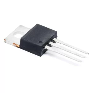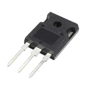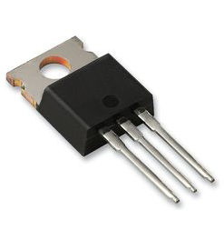



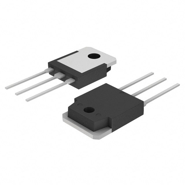
2SK2361 N-Channel Power MOSFET 450V 10A TO-3P
2SK2361 N-Channel Power MOSFET, 450V, 10A DC, RDS(on) 0.9Ω— designed for high-voltage industrial switching applications.
20.00 EGP
In stockSKU 3496300160693
Buy Now
Shipping across EgyptDelivered to your door
Cash on deliveryPay when your order arrives
Not sure it fits your project?Ask us on WhatsApp - we reply fast
2SK2361 N-Channel Power MOSFET 450V 10A TO-3P
The 2SK2361 is an N-Channel MOS Field Effect Transistor (Power MOS FET) manufactured by NEC Corporation, designed for high-voltage switching applications and rated for industrial use. The device blocks up to 450 V drain-to-source (VDSS) and handles a DC drain current of ±10 A (±40 A pulsed), with a total power dissipation of 100 W at a case temperature of 25 °C (3.0 W at 25 °C ambient).
It combines low on-resistance — RDS(on) of only 0.9 Ω maximum at VGS = 10 V, ID = 5.0 A — with low typical input capacitance (Ciss = 1050 pF) for fast, efficient switching, and high avalanche capability ratings (single avalanche current IAS = 10 A, single avalanche energy EAS = 142 mJ). A diode connected between gate and source serves as protection against ESD. The transistor is supplied in the MP-88 package, in which the metal fin (pin 4) is connected to the drain. The same datasheet also covers the companion device 2SK2362 (VDSS = 500 V, RDS(on) = 1.0 Ω max.).
Features
- N-Channel MOS field effect transistor for high-voltage switching (industrial use)
- Low on-resistance: RDS(on) = 0.9 Ω max. (VGS = 10 V, ID = 5.0 A)
- Low input capacitance: Ciss = 1050 pF typ.
- High avalanche capability ratings (IAS = 10 A, EAS = 142 mJ)
- High voltage blocking: VDSS = 450 V; VGSS = ±30 V
- High current capability: ID = ±10 A (DC), ±40 A (pulse)
- Power dissipation: 100 W (TC = 25 °C) / 3.0 W (TA = 25 °C)
- Fast switching: td(on) = 15 ns, tr = 24 ns, td(off) = 50 ns, tf = 14 ns (typ.)
- Low total gate charge: QG = 26 nC (typ.)
- Built-in gate–source diode for ESD protection
Specifications
Absolute Maximum Ratings (TA = 25°C)
| Parameter | Symbol | Rating | Unit | Conditions / Notes |
|---|---|---|---|---|
| Drain to Source Voltage | VDSS | 450 | V | 2SK2361 (companion 2SK2362: 500 V) |
| Gate to Source Voltage | VGSS | ±30 | V | |
| Drain Current (DC) | ID (DC) | ±10 | A | |
| Drain Current (Pulse) | ID (pulse) | ±40 | A | PW ≤ 10 µs, Duty Cycle ≤ 1 % |
| Total Power Dissipation | PT1 | 100 | W | TC = 25 °C |
| Total Power Dissipation | PT2 | 3.0 | W | TA = 25 °C |
| Channel Temperature | Tch | 150 | °C | |
| Storage Temperature | Tstg | -55 to +150 | °C | |
| Single Avalanche Current | IAS | 10 | A | Starting Tch = 25 °C, RG = 25 Ω, VGS = 20 V → 0 |
| Single Avalanche Energy | EAS | 142 | mJ | Starting Tch = 25 °C, RG = 25 Ω, VGS = 20 V → 0 |
Electrical Characteristics (TA = 25°C)
| Characteristic | Symbol | Min. | Typ. | Max. | Unit | Test Conditions |
|---|---|---|---|---|---|---|
| Drain to Source On-Resistance | RDS(on) | – | 0.7 | 0.9 | Ω | VGS = 10 V, ID = 5.0 A |
| Gate to Source Cutoff Voltage | VGS(off) | 2.5 | – | 3.5 | V | VDS = 10 V, ID = 1 mA |
| Forward Transfer Admittance | |yfs| | 3.0 | – | – | S | VDS = 10 V, ID = 5.0 A |
| Drain Leakage Current | IDSS | – | – | 100 | µA | VDS = VDSS, VGS = 0 |
| Gate to Source Leakage Current | IGSS | – | – | ±100 | nA | VGS = ±30 V, VDS = 0 |
| Input Capacitance | Ciss | – | 1050 | – | pF | VDS = 10 V, VGS = 0, f = 1 MHz |
| Output Capacitance | Coss | – | 200 | – | pF | VDS = 10 V, VGS = 0, f = 1 MHz |
| Reverse Transfer Capacitance | Crss | – | 26 | – | pF | VDS = 10 V, VGS = 0, f = 1 MHz |
| Turn-On Delay Time | td(on) | – | 15 | – | ns | ID = 5.0 A, VGS = 10 V, VDD = 150 V, RG = 10 Ω, RL = 30 Ω |
| Rise Time | tr | – | 24 | – | ns | ID = 5.0 A, VGS = 10 V, VDD = 150 V, RG = 10 Ω, RL = 30 Ω |
| Turn-Off Delay Time | td(off) | – | 50 | – | ns | ID = 5.0 A, VGS = 10 V, VDD = 150 V, RG = 10 Ω, RL = 30 Ω |
| Fall Time | tf | – | 14 | – | ns | ID = 5.0 A, VGS = 10 V, VDD = 150 V, RG = 10 Ω, RL = 30 Ω |
| Total Gate Charge | QG | – | 26 | – | nC | ID = 10 A, VDD = 400 V, VGS = 10 V |
| Gate to Source Charge | QGS | – | 6.1 | – | nC | ID = 10 A, VDD = 400 V, VGS = 10 V |
| Gate to Drain Charge | QGD | – | 12 | – | nC | ID = 10 A, VDD = 400 V, VGS = 10 V |
| Body Diode Forward Voltage | VF (S-D) | – | – | 1.0 | V | IF = 10 A, VGS = 0 |
| Reverse Recovery Time | trr | – | 350 | – | ns | IF = 10 A, VGS = 0, di/dt = 50 A/µs |
| Reverse Recovery Charge | Qrr | – | 2.0 | – | µC | IF = 10 A, VGS = 0, di/dt = 50 A/µs |

Applications
- High-voltage switching circuits
- Switching power supplies
- Industrial equipment (machine tools, industrial robots)
- Computers, office equipment, communications equipment
- Test and measurement equipment
- Audio and visual equipment, home electronic appliances
Package Content
- 1 x 2SK2361 N-Channel Power MOSFET 450V 10A TO-3P
DataSheet
Related products