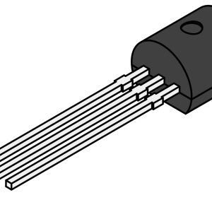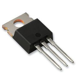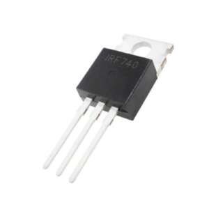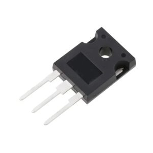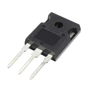


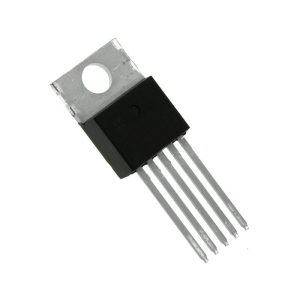









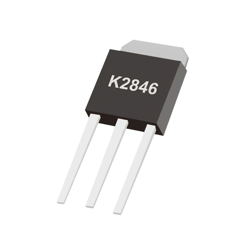
Toshiba 2SK2846 N-Channel MOSFET Transistor 600V 2A 2-8M1B
Toshiba 2SK2846 N-channel through-hole MOSFET (600V, 2A). Features low ON resistance (4.2Ω typ) for efficient switching in DC-DC converters and motor drives.
20.00 EGP
In stockSKU 34963001511110
Buy Now
Shipping across EgyptDelivered to your door
Cash on deliveryPay when your order arrives
Not sure it fits your project?Ask us on WhatsApp - we reply fast
Toshiba 2SK2846 N-Channel MOSFET Transistor 600V 2A 2-8M1B
The 2SK2846 is a high-performance, silicon N-channel MOS type field effect transistor. It features an advanced enhancement-mode structure designed to handle a maximum drain-source voltage of 600V and a continuous DC drain current of up to 2A. This transistor is highly efficient and optimized for power management and switching environments.
Features
- Low Drain-Source ON Resistance
- High Forward Transfer Admittance
- Low Leakage Current
- Enhancement-Mode
Specifications
Absolute Maximum Ratings (Ta = 25°C)
| Characteristic | Symbol | Rating | Unit |
|---|---|---|---|
| Drain-Source Voltage | VDSS | 600 | V |
| Drain-Gate Voltage (RGS = 20 kΩ) | VDGR | 600 | V |
| Gate-Source Voltage | VGSS | ±30 | V |
| Drain Current (DC) (Note 1) | ID | 2 | A |
| Drain Current (Pulse, t = 1 ms) (Note 1) | IDP | 5 | A |
| Drain Current (Pulse, t = 100 μs) (Note 1) | IDF | 8 | A |
| Drain Power Dissipation | PD | 1.3 | W |
| Single Pulse Avalanche Energy (Note 2) | EAS | 93 | mJ |
| Avalanche Current | IAR | 2 | A |
| Repetitive Avalanche Energy (Note 3) | EAR | 0.13 | mJ |
| Channel Temperature | Tch | 150 | °C |
| Storage Temperature Range | Tstg | -55 ~ 150 | °C |
Thermal Characteristics
| Characteristic | Symbol | Max | Unit |
|---|---|---|---|
| Thermal Resistance, Channel to Ambient | Rth(ch-a) | 96.1 | °C/W |
Electrical Characteristics (Ta = 25°C)
| Characteristic | Symbol | Test Condition | Min | Typ. | Max | Unit |
|---|---|---|---|---|---|---|
| Gate Leakage Current | IGSS | VGS = ±25 V, VDS = 0 V | — | — | ±10 | μA |
| Gate-Source Breakdown Voltage | V(BR)GSS | ID = ±10 μA, VGS = 0 V | ±30 | — | — | V |
| Drain Cut-off Current | IDSS | VDS = 600 V, VGS = 0 V | — | — | 100 | μA |
| Drain-Source Breakdown Voltage | V(BR)DSS | ID = 10 mA, VGS = 0 V | 600 | — | — | V |
| Gate Threshold Voltage | Vth | VDS = 10 V, ID = 1 mA | 2.0 | — | 4.0 | V |
| Drain-Source ON Resistance | RDS(ON) | VGS = 10 V, ID = 1 A | — | 4.2 | 5.0 | Ω |
| Forward Transfer Admittance | |Yfs| | VDS = 10 V, ID = 1 A | 0.8 | 1.7 | — | S |
| Input Capacitance | Ciss | VDS = 10 V, VGS = 0 V, f = 1 MHz |
— | 380 | — | pF |
| Reverse Transfer Capacitance | Crss | — | 40 | — | pF | |
| Output Capacitance | Coss | — | 120 | — | pF | |
| Rise Time | tr | VDD ≈ 200 V, ID = 1 A, RL = 200 Ω, VGS = 10 V, Duty ≤ 1%, tw = 10 μs |
— | 15 | — | ns |
| Turn-on Time | ton | — | 25 | — | ns | |
| Fall Time | tf | — | 20 | — | ns | |
| Turn-off Time | toff | — | 80 | — | ns | |
| Total Gate Charge | Qg | VDD ≈ 480 V, VGS = 10 V, ID = 2 A |
— | 9 | — | nC |
| Gate-Source Charge | Qgs | — | 5 | — | nC | |
| Gate-Drain (“Miller”) Charge | Qgd | — | 4 | — | nC |
Source-Drain Diode Ratings and Characteristics (Ta = 25°C)
| Characteristic | Symbol | Test Condition | Min | Typ. | Max | Unit |
|---|---|---|---|---|---|---|
| Continuous Drain Reverse Current | IDR | — | — | — | 2 | A |
| Pulse Drain Reverse Current (t = 1 ms) | IDRP | — | — | — | 5 | A |
| Pulse Drain Reverse Current (t = 100 μs) | IDRP | — | — | — | 8 | A |
| Forward Voltage (Diode) | VDSF | IDR = 2 A, VGS = 0 V | — | — | -1.5 | V |
| Reverse Recovery Time | trr | IDR = 2 A, VGS = 0 V, dIDR/dt = 100 A/μs |
— | 1000 | — | ns |
| Reverse Recovery Charge | Qrr | — | 3.5 | — | μC |
Applications
- Chopper Regulators
- DC-DC Converters
- Motor Drive Applications
- General power switching in computer, office, industrial, and domestic appliances
Package Content
- 1 x Toshiba 2SK2846 N-Channel MOSFET Transistor 600V 2A 2-8M1B
DataSheet
Related products